

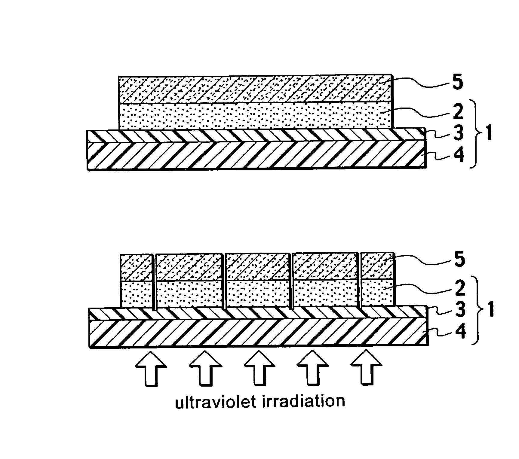
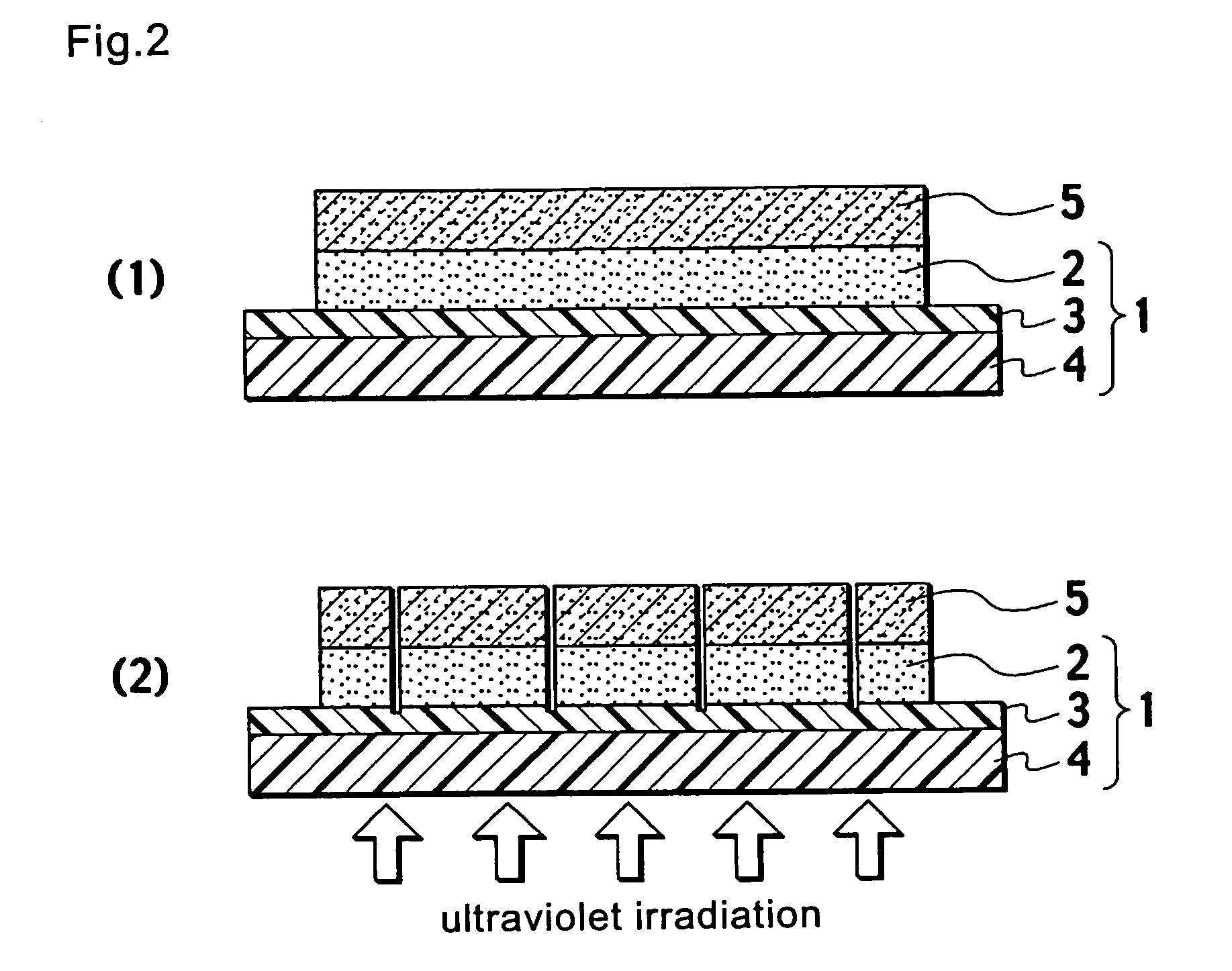
Dicing/die bonding sheet
a technology of die bonding and die bonding, which is applied in the direction of heat-activated film/foil adhesives, film/foil adhesives, synthetic resin layered products, etc., can solve the problems that film adhesives and dicing tapes may not separate satisfactorily, and achieve satisfactory adhesiveness.
- Summary
- Abstract
- Description
- Claims
- Application Information
AI Technical Summary
Benefits of technology
Problems solved by technology
Method used
Image

Examples
examples
[0095] As follows is a more detailed description of the present invention based on a series of examples, although the present invention is in no way limited by the examples presented below.
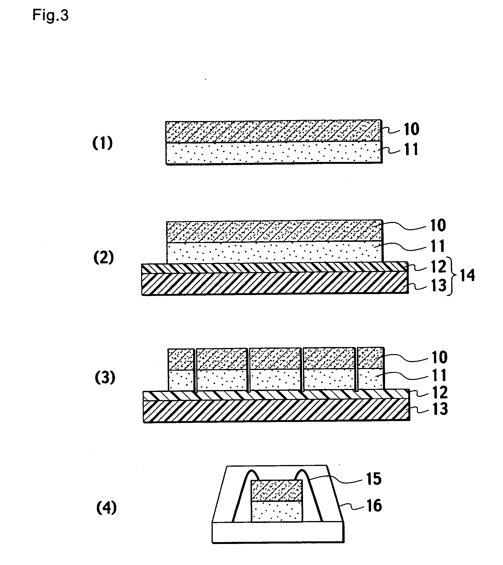
[0096] Radiation curable pressure-sensitive adhesives were prepared as described below in examples 1 to 6 and comparative examples 1 to 3, and were each then applied to an ethylene-vinyl acetate copolymer film in the manner described below, thus forming an adhesive tape. Subsequently, an adhesive film prepared in advance in the manner described below was laminated to the pressure-sensitive adhesive layer of the adhesive tape, yielding a dicing / die bonding sheet.
[0097] The properties of the dicing / die bonding sheets prepared in this manner were tested and evaluated. These properties were evaluated in the following manner.
1) Peel Strength
[0098] This is an indicator of the ease with which the laminated adhesive film and adhesive tape are able to be peeled apart. Prior to ultraviolet irradiation,...
examples 1 to 6
[0111] Samples of the adhesive film 1 were laminated to the adhesive tapes described above to prepare the dicing / die bonding sheets of the examples 1 to 6 and the comparative examples 1 to 3 shown in Table 1, and the properties of these sheets were then evaluated.
[0112] As shown in the examples 1 through 6, with the dicing / die bonding sheets prepared by laminating the adhesive film 1 to an adhesive tape produced using one of the pressure-sensitive adhesive compositions 1 to 6, irradiation following dicing causes a satisfactory reduction in the peel strength of the pressure-sensitive adhesive layer, meaning during pickup, the structure separates between the pressure-sensitive adhesive layer and the adhesive layer, resulting in a favorable pickup success rate. Furthermore, with these dicing / die bonding sheets, even if the entire dicing / die bonding sheet is irradiated following dicing, a satisfactory spacing can still be retained between elements when the dicing / die bonding sheet is s...
PUM
| Property | Measurement | Unit |
|---|---|---|
| glass transition temperature | aaaaa | aaaaa |
| particle diameter | aaaaa | aaaaa |
| heat resistance | aaaaa | aaaaa |
Abstract
Description
Claims
Application Information