Technique to improve the gain and signal to noise ratio in CMOS switched capacitor amplifiers

Inactive Publication Date: 2007-02-08
MICRON TECH INC
View PDF14 Cites 4 Cited by
  • Summary
  • Abstract
  • Description
  • Claims
  • Application Information

AI Technical Summary

Benefits of technology

[0016] Another exemplary embodiment of the present invention includes a method of amplifying a signal. The method comprises coupling a reference voltage to an inverting input of a CMOS amplifier and coupling an input signal, through a switched feed-in capacitance, to a non-inverting input of the CMOS amplifier. The method further comprises amplifying the non-inverting input using the CMOS amplifier to generate an amplifier output and feeding back the amplifier output, through a switched feedback capacitance, to the non-inverting input. The switched feedback capacitance and the switched feed-in capacitance may be selected to maintain a stable gain of the CMOS amplifier and increase a signal-to-noise ratio of the CMOS amplifier.
[0017] Yet another exemplary embodim

Problems solved by technology

However, in these digital circuits, the positive feedback gain is very large and the circuit is inherently unstable.
Furthermore, positive feedback digital amplifiers generally produce a large non-linear output voltage, which is often limited by the power supply voltage

Method used


Image

  • Technique to improve the gain and signal to noise ratio in CMOS switched capacitor amplifiers
  • Technique to improve the gain and signal to noise ratio in CMOS switched capacitor amplifiers
  • Technique to improve the gain and signal to noise ratio in CMOS switched capacitor amplifiers

Examples


Embodiment Construction

[0036] The present invention comprises switched capacitor amplifiers including positive feedback and methods for amplifying signals using positive feedback, while maintaining a stable gain and producing an improved signal-to-noise ratio.

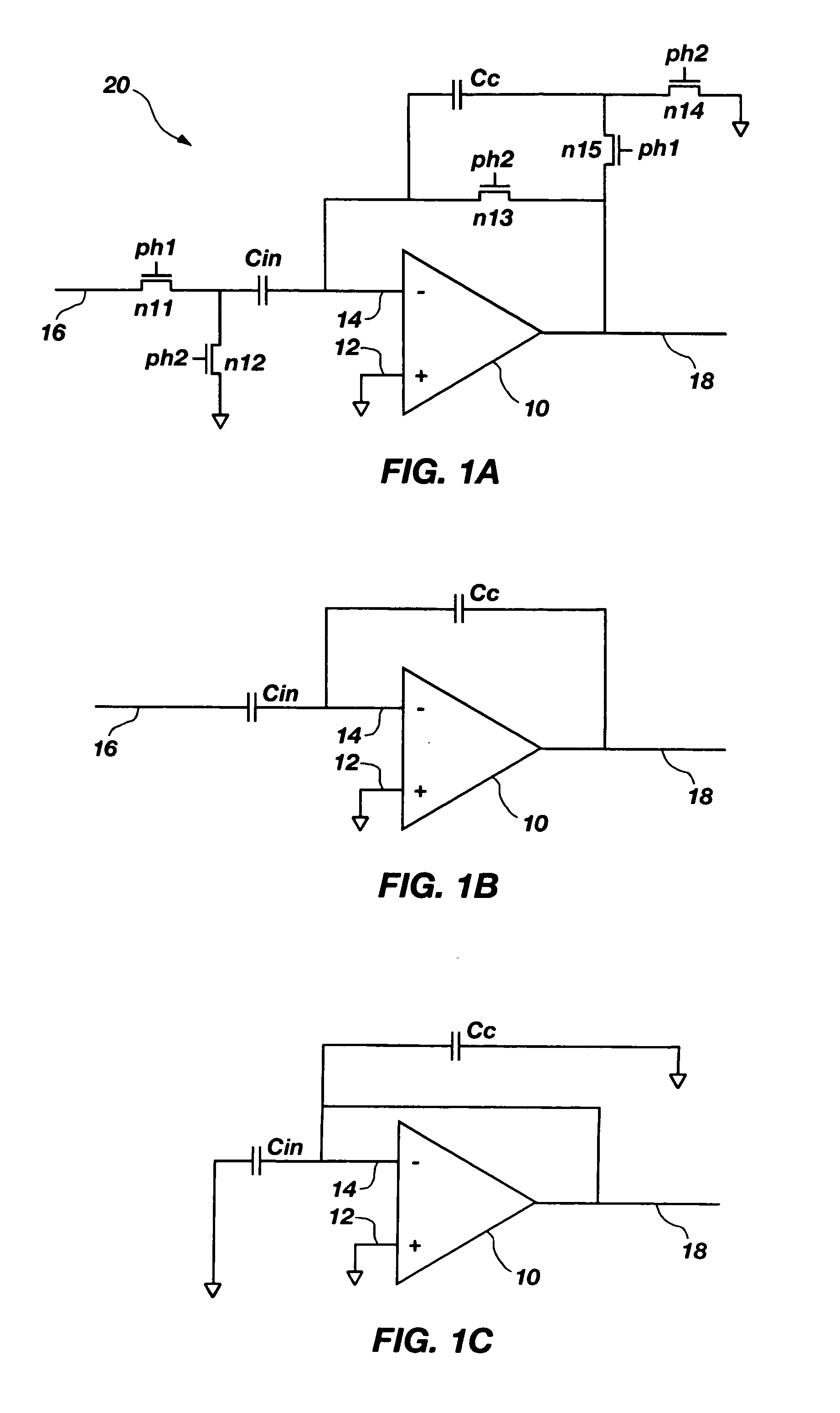
[0037] As stated earlier, FIG. 1A illustrates a conventional switched capacitor amplifier 20 with negative feedback. During the gain phase, the switched capacitor amplifier 20 performs an amplifying function with a gain that can be approximated by −Cin / Cc). However, any input offset voltage across the feed-in capacitor Cin and the feedback capacitor Cc may build up charge, causing the input offset voltage to be amplified, and may eventually cause the amplifier output 18 to become saturated when it nears the positive or negative voltage sources, which may cause the amplified output to be clipped. To correct this charge buildup, the reset phase discharges any buildup and the gain stage can again operate accurately. In addition, canceling the input off...


PUM


Abstract

The present invention comprises switched capacitor amplifiers including positive feedback, semiconductor devices, wafers and systems incorporating same and methods for amplifying signals using positive feedback, while maintaining a stable gain and producing an improved signal-to-noise ratio. One embodiment includes a switched capacitor amplifier comprising a Complementary Metal Oxide Semiconductor (CMOS) amplifier, a feed-in switched capacitor, and a feedback switched capacitor. The feed-in switched capacitor operably couples an input signal to the non-inverting input of the CMOS amplifier. Similarly, the feedback switched capacitor operably couples the amplifier output to the non-inverting input to create a positive feedback loop. A capacitance of the feedback switched capacitor relative to a capacitance of the feed-in switched capacitor comprises a feedback proportion. This feedback proportion may be configured to maintain a stable gain of the switched capacitor amplifier and increase a signal-to-noise ratio of the switched capacitor amplifier, even with the switched capacitor amplifier configured in a positive feedback arrangement.

Description

BACKGROUND OF THE INVENTION [0001] 1. Field of the Invention [0002] The present invention relates to amplifier circuits. More specifically, the present invention relates to switched capacitor CMOS amplifiers and operation thereof. [0003] 2. Description of Related Art [0004] Many systems that manipulate and generate analog signals require amplification of those signals for presentation to other circuitry within the system. In Dynamic Random Access Memories (DRAM), as well as other semiconductor devices, amplifiers may be required in operational blocks such as sense amplifiers, input signal level sensors, phase locked loops, delay locked loops, general sensors, and various other analog circuits. [0005] Regenerative receivers were first widely used in vacuum tube radio receivers. They provided a large signal gain, increased selectivity, an improved signal-to-noise ratio, and enabled the first widespread use of radio communication. This was accomplished with a minimal number of componen...

Claims


Application Information

Patent Timeline
IPC IPC(8): H03F1/02
CPCH03F1/26H03F1/38H03F3/005H03F3/45183H03F2203/45722H03F2203/45224H03F2203/45514H03F2203/45551H03F2203/45674H03F2203/45166
Inventor FORBES, LEONARDCUTHBERT, DAVID R.
Owner MICRON TECH INC
Why Eureka
Try Eureka