Manufacture method for micro structure

a manufacturing method and micro-structure technology, applied in the field of manufacturing methods for micro-structures, can solve the problems of resist pattern falling, resist material mainly used is photosensitive to a short wavelength of 193 nm but not stable, resist is not so stable, etc., to achieve easy etching, good controllability, and patterning. easy

Inactive Publication Date: 2007-02-15
FUJITSU LTD
View PDF0 Cites 225 Cited by
  • Summary
  • Abstract
  • Description
  • Claims
  • Application Information

AI Technical Summary

Benefits of technology

[0014] (d) after said step (c), removing said resist pattern; (e) after said step (d), thinning said upper hard mask by etching; (f) etching said lower hard mask film by using said thinned upper hard mask as an etching mask to form a lower hard mask; and (g) etching said etching target film by using said upper hard mask and said lower hard mask as an etching mask, wherein said upper hard mask film is capable of being more easily etched, using said resist pattern as a mask, than said lower hard mask film.
[0015] The resist pattern is used as a mask for etching the upper hard mask. The upper hard mask can be pattern...

Problems solved by technology

This Publication points out the problems that at the exposure wavelength of 193 nm, resist is not so stable, edge roughness having coarse pattern lines increases, a resist film thickness after trim...

Method used


Image

  • Manufacture method for micro structure
  • Manufacture method for micro structure
  • Manufacture method for micro structure

Examples


first embodiment

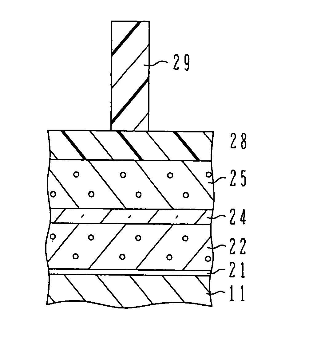
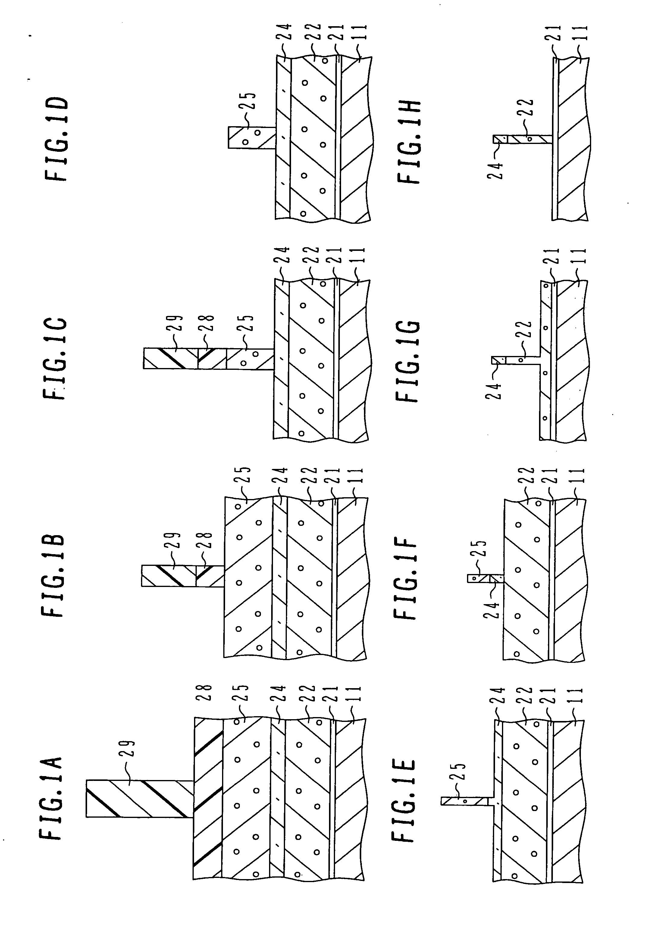
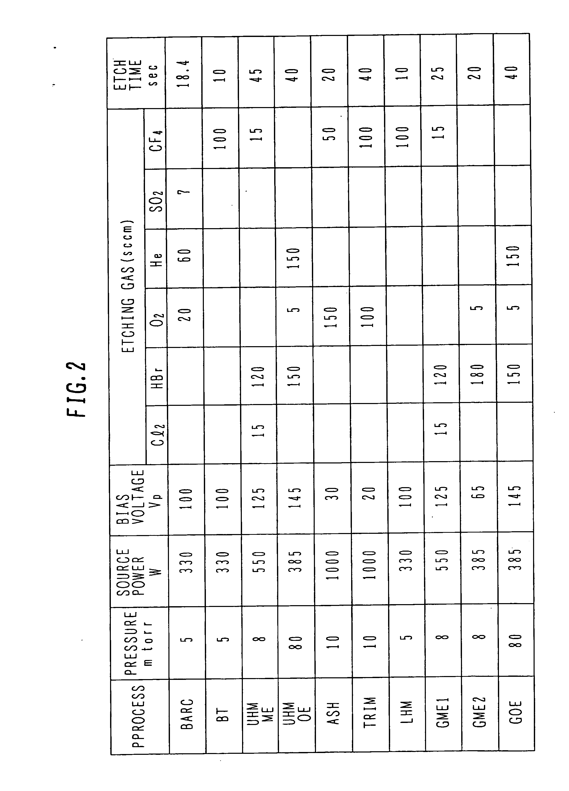
[0032] With reference to FIGS. 1A to 1H, the first embodiment will be described. FIGS. 1A to 1H are cross sectional views of a semiconductor substrate illustrating main processes of a micro structure manufacture method. A series of etching / trimming processes is executed by using, for example, an inductively coupled plasma (ICP) etcher. A table in FIG. 2 shows a summary of process conditions.

[0033] As shown in FIG. 1A, the surface of a silicon substrate 11 is thermally oxidized and nitrogen or the like is introduced to form a silicon oxynitride film 21 having a thickness of about 1 nm, the silicon oxynitride film constituting a gate insulating film. A polysilicon film 22 constituting gate electrodes is deposited on the gate insulating film 21 to a thickness of 105 nm by thermal CVD. The polysilicon film 22 is an etching target film. A silicon oxide film 24 as a lower hard mask film is deposited on the polysilicon film 22 to a thickness of 30 nm by thermal CVD, and a polysilicon film ...

second embodiment

[0067]FIGS. 6A to 6D are cross sectional views of a semiconductor substrate illustrating main processes of a micro structure manufacture method according to the

[0068] As shown in FIG. 6A, a gate insulating film 21 of HfSiON having a thickness of 5 nm is formed on the surface of a silicon substrate. A TiN layer 22a having a thickness of 10 nm and a W layer 22b having a thickness of 70 nm are stacked on the gate insulating film by CVD or sputtering (PVD) to form a gate electrode layer.

[0069] For example, the HfSiON film 21 is formed by thermally oxidizing the surface of the silicon substrate and growing an HfON film on silicon oxide by CVD. Nitrogen may be introduced after thermal oxidation. The HfSiON film may be grown by CVD. By using material having a dielectric constant higher than that of silicon oxide, the physical thickness of the gate insulating film can be made thick while a silicon oxide equivalent thickness is maintained low, and leakage current can be suppressed. The mate...

third embodiment

[0076]FIGS. 7A to 7D are cross sectional views of a semiconductor substrate illustrating the main processes of a micro structure manufacture method according to the

[0077] As shown in FIG. 7A, a polysilicon film 22b having a thickness of 100 nm is formed on a TaN layer 22a having a thickness of 5 nm to form a gate electrode layer. The TaN layer is deposited by sputtering (reactive sputtering). Other lamination structures are similar to those of the first embodiment.

[0078]FIG. 7B shows the state that a hard mask is formed, corresponding to FIG. 1F. The silicon surface of the upper gate electrode layer 22b is exposed.

[0079]FIG. 7C shows the state that the polysilicon gate electrode 22b is etched by using mixture gas of HBr / O2 similar to the process shown in FIG. 1G. The TaN lower gate electrode 22a functions as an etch stopper. Even if the upper hard mask of polysilicon is left, it can be removed at this stage by over-etching.

[0080]FIG. 7D shows the state that the lower gate electro...


PUM


Abstract

A micro structure manufacture method includes the steps of: (a) preparing an etching object having an etching target film, provided with a lower hard mask layer and an upper hard mask layer stacked on the etching target film; (b) forming a resist pattern above the etching object; (c) etching the upper hard mask film by using the resist pattern as an etching mask to form an upper hard mask; (d) after the step (c), removing the resist pattern; (e) after the step (d), thinning the upper hard mask by etching; (f) etching the lower hard mask film by using the thinned upper hard mask as an etching mask to form a lower hard mask; and (g) etching the etching target film by using the upper hard mask and the lower hard mask as an etching mask, wherein the upper hard mask film is capable of being more easily etched, using the resist pattern as a mask, than the lower hard mask film. The micro structure manufacture method can etch a fine pattern with good yield.

Description

CROSS REFERENCE TO RELATED APPLICATION [0001] This application is based on and claims priority of Japanese Patent Application No. 2005-235435 filed on Aug. 15, 2005, the entire contents of which are incorporated herein by reference. BACKGROUND OF THE INVENTION [0002] A) Field of the Invention [0003] The present invention relates to a manufacture method for a micro structure, and more particularly to a manufacture method for a micro structure having a pattern narrower than the minimum size of a resist pattern exposed and developed. [0004] B) Description of the Related Art [0005] The current processing of semiconductor devices generally uses techniques of etching various films such as silicon films, silicon oxide films, and silicon nitride films by reactive ion etching (RIE) using a resist pattern formed by lithography. A light source of photolithography has changed from KrF excimer laser (wavelength 248 nm) to ArF excimer laser (wavelength 193 nm) to form finer resist patterns. Resis...

Claims


Application Information

Patent Timeline
IPC IPC(8): G03F7/26
CPCH01L21/0338H01L21/28088H01L21/28123H01L21/31116H01L21/31138H01L21/32136H01L29/518H01L21/32139H01L21/823842H01L29/495H01L29/4966H01L29/517H01L21/32137
Inventor MORIOKA, HIROSHI
Owner FUJITSU LTD
Why Eureka
Try Eureka