Rapid thermal annealing of targeted thin film layers

Inactive Publication Date: 2007-02-15
NANOSCALE COMPONENTS
View PDF10 Cites 33 Cited by
  • Summary
  • Abstract
  • Description
  • Claims
  • Application Information

AI Technical Summary

Benefits of technology

[0014] In accordance with an embodiment, the method includes providing, on a substrate, a plurality of thin film layers. The layers, in one embodiment, may include metals or metal oxides, such as SBT, BST, BLT, PZT, or other multiple or single metal materials. Next, a first temperature range sufficient to anneal a targeted layer on the substrate may be generated. The first temperature range may be from about 400° C. to about 1000° C. Once generated, the targeted layer may be exposed to the first temperature range, for a predetermined time period less than that necessary to render the targeted layer substantially annealed, so as to minimize exposure of the remaining layers to the first temperature range. Exposure may be for a few milliseconds to a pulse or a flash of heat energy. By minimizing exposure of the remaining layers to the first temperature range damages to the remaining layers can be avoided. Thereafter, the targeted layer may be cooled to a second temperature range below that of the first temperature range. For instance, the second temperature range may be about half of the first temperature range. Subsequently, the substrate may be re-exposed to the first temperature range, for the predetermined time period, to reheat the targeted layer toward the first temperature range. The re-exposure permits additional energy to be absorbed into the targeted layer to further increase its thermal profile towards the temperature that permit subsequent annealing of the targeted layer.
[0015] In accordance with another embodiment of the present invention, a method is provided for annealing a targeted layer on a substrate. The method includes initially pre-heating a substrate having a plurality of overlapping thin film layers to an intermediate temperature. Next, a rapid pulse of heat energy at a first temperature range higher than the intermediate temperature and sufficient to anneal a targeted layer may be emitted toward a targeted layer. The pulse of heat energy, in an embodiment, is only for a predetermined time period less than that necessary to render the targeted layer substantially annealed. As su

Problems solved by technology

In addition, as the density increases, power consumption and electrical current requirements have also increased.
However, many of the required capacitors (currently planar) have grown in size to a point that they can no longer fit onto the IC chip.
The farther away the decoupling capacitor is mounted from the LSI chip, however, the worse the overall performance of the connecting “wires.” If the decoupling capacitors could be mounted on the chip or even on the intermediate chip mount at low cost, then printed circuit board space and overall cost could be greatly reduced.
However, although the relative dielectric strength of these materials can help reduce the feature size of the capacitor, such can limit, for instance, the compatibility of the new materials.
When targeting, for instance, only an upper layer for annealing, exposure of the underlying layers, along with other FETs and interconnects, to similar heating conditions can damage the underlying layers and compromise the performance of the underlying layers.
As IC dimensional design shrink, exposure of underlying layers to conditions necessary to complete the annealing process in the top layer, even at a low thermal budget, can compromise the integrity of the underlying layers.
Other types of etching, such as elect

Method used


Image

  • Rapid thermal annealing of targeted thin film layers
  • Rapid thermal annealing of targeted thin film layers
  • Rapid thermal annealing of targeted thin film layers

Examples


Embodiment Construction

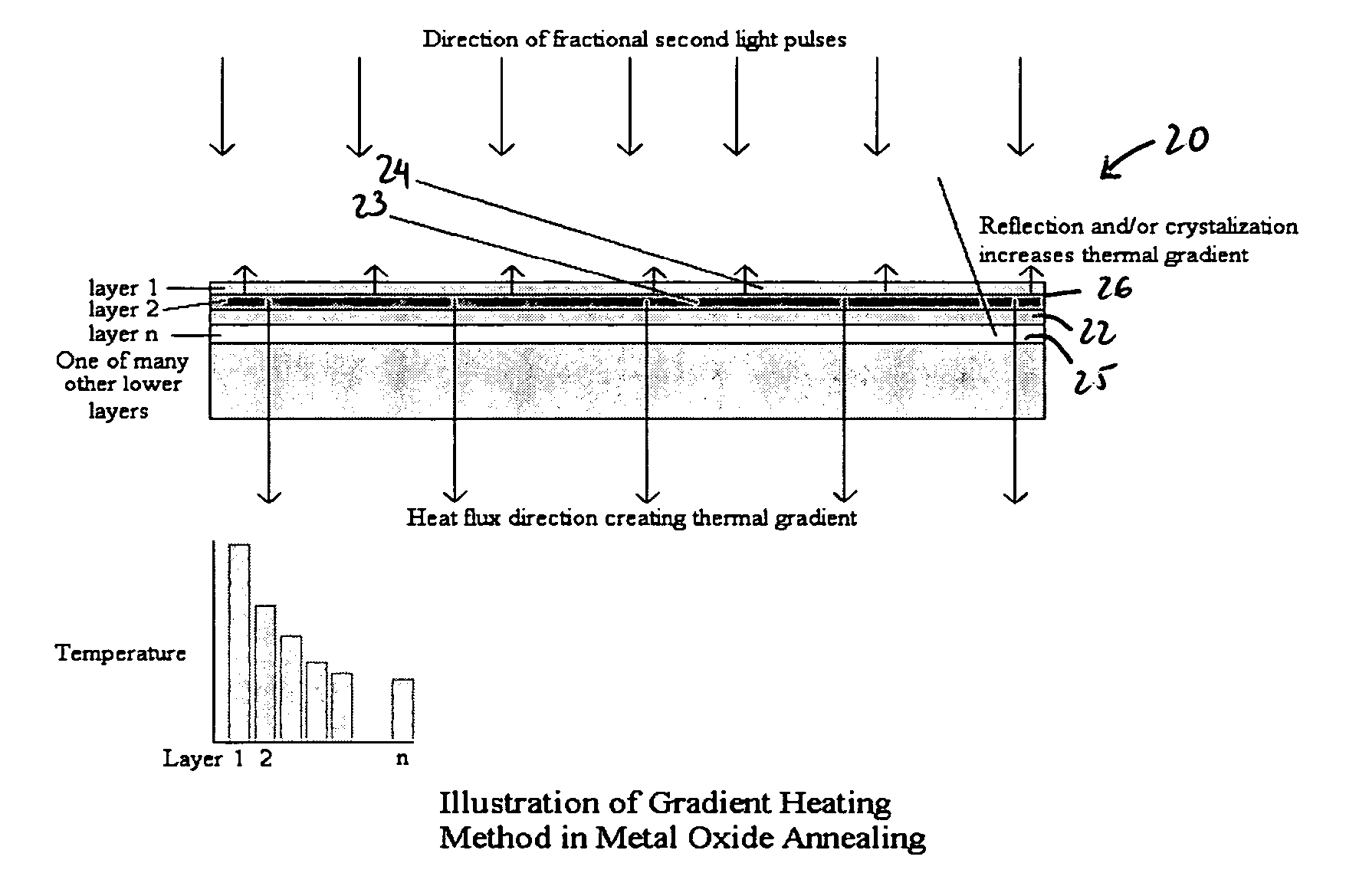
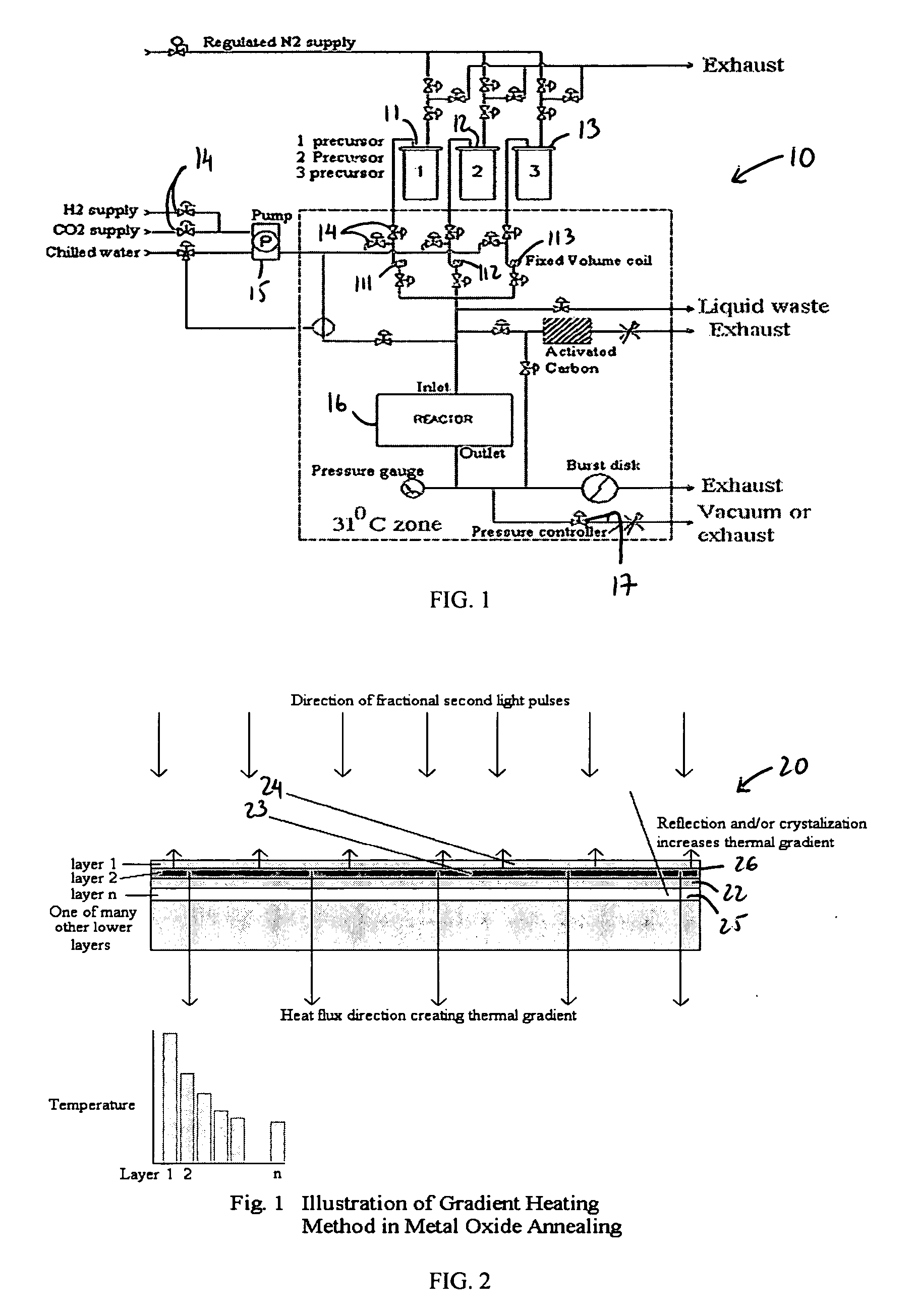
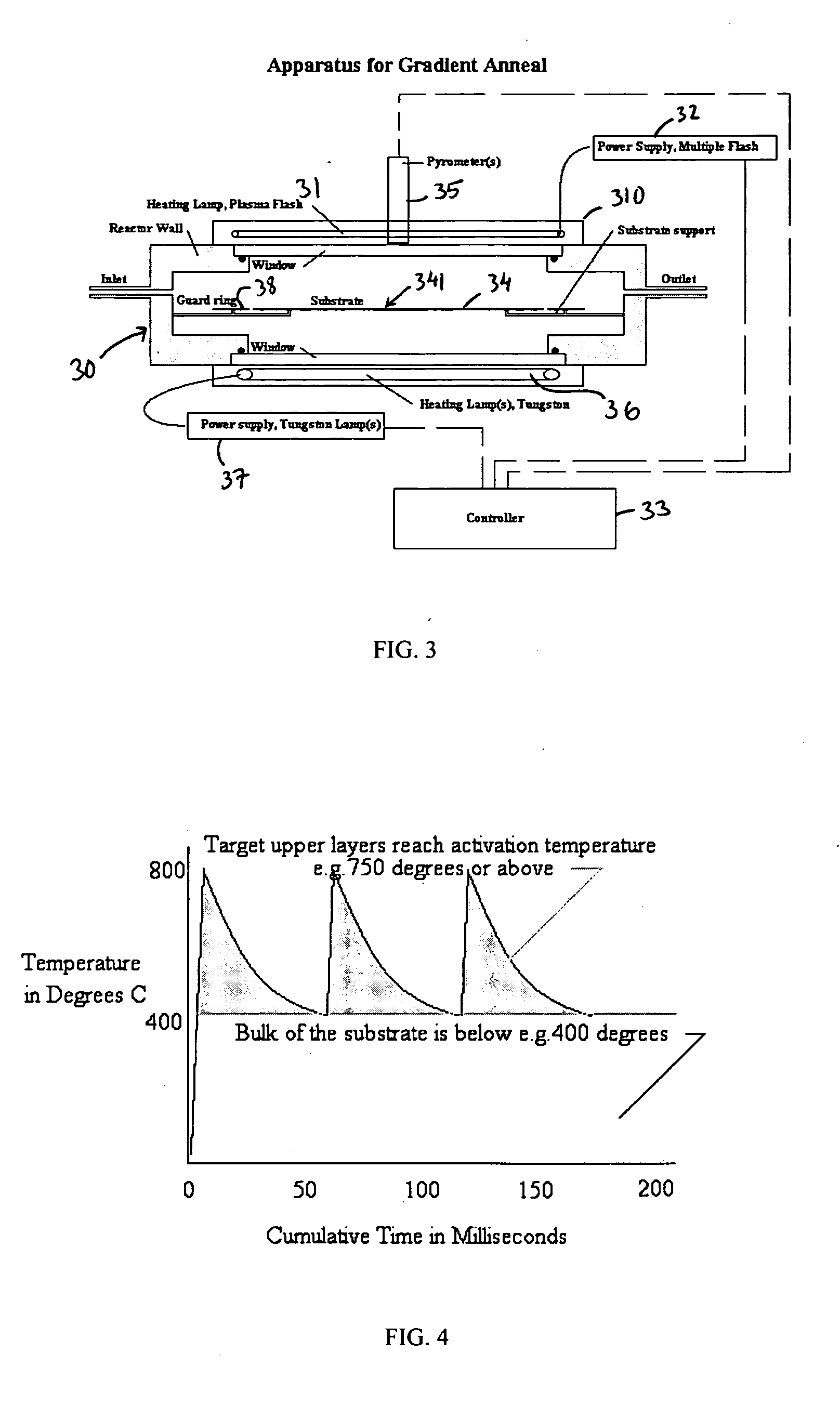
[0023] The present invention provides, in one embodiment, a rapid thermal annealing (RTA) method for use in connection with the fabrication of a capacitor whereby an upper thin film or layer (i.e., targeted layer) of an integrated circuit may be heated to a desired temperature range, while exposure of the underlying layers to such a temperature range may be minimized, so as to avoid damage to the underlying layers.

[0024] In accordance with one embodiment of the present invention, the RTA method involves the use of, for example, impulse, flash-assist or laser anneal, subsequent to the deposition of a metal or metal oxide as barrier layers (e.g., oxides of Ru, Pd, Ti, Ta, etc.), dielectrics and perovskites (e.g., oxides of Al, Ta, Hf, SBT, BLT, BST, PZT etc.), and / or conductors (e.g., Pt, Ru, Ir, Cu etc.). The use of such an annealing procedure enables a thermal ramp rate to be controlled at a substantially fast rate, such that the bulk of the substrate lags significantly behind a ta...


PUM


Abstract

A method for rapid thermal annealing of thin film layers is provided. The method directs a series of pulses or flashes of heat energy toward a targeted layer on a substrate. Each pulse may be at a first temperature range sufficient to anneal the targeted layer, but has a duration that is less than that necessary to render the targeted layer substantially annealed. Moreover, in succession, the series of pulses can incrementally raise the targeted layer to a temperature sufficient for annealing, while minimizing exposure of the remaining layers to the pulses of heat energy. A reactor for implementing the rapid thermal annealing process is also provided.

Description

RELATED US APPLICATION(S) [0001] The present application claims priority to U.S. Provisional Patent Application Ser. No. 60 / 696,049, filed Jun. 30, 2005, and is a continuation-in-part of U.S. patent application Ser. No. 11 / 358,343, filed Feb. 21, 2006, both of which are hereby incorporated herein by reference.TECHNICAL FIELD [0002] The present invention relates to methods of annealing targeted thin film layers on a substrate, and more particularly, to a rapid thermal annealing process while maintaining a gradient of temperature across different layers. BACKGROUND ART [0003] New techniques in patterning and deposition have led the way in fulfilling Moore's Law (the historical increase in processor speed), as well as the trend toward lower cost via smaller feature sizes and denser circuitry. Over the history of Large Scale Integrated (LSI) circuits, transistor density has increased dramatically to the extent that as the scale of construction has been halved, the density of transistors...

Claims


Application Information

Patent Timeline
IPC IPC(8): H01L21/8242H01L21/4763
CPCH01G4/33H01G13/04H01L28/55H01L21/31691H01L21/76838H01L21/288H01L21/02197H01L21/02282H01L21/02318
Inventor GRANT, ROBERT W.
Owner NANOSCALE COMPONENTS
Why Eureka
Try Eureka