Solid-state imager and formation method using anti-reflective film for optical crosstalk reduction

a technology of anti-reflective film and solid-state imager, which is applied in the direction of electrical equipment, semiconductor devices, radio frequency controlled devices, etc., can solve the problem of disadvantageous high light reflection of aluminum, and achieve the effect of reducing optical crosstalk

Inactive Publication Date: 2007-03-01
MICRON TECH INC
View PDF6 Cites 59 Cited by
  • Summary
  • Abstract
  • Description
  • Claims
  • Application Information

AI Technical Summary

Benefits of technology

[0013] In an exemplary embodiment of the invention, pixel arrays with conductive lines having reflecting surfaces with the potential to produce optical crosstalk in pixel circuits are coated with an anti-reflective film. The anti-reflective film is disposed between the reflecting surface and an over-lying insulating layer to produce a first interface between the anti-reflective film and the insulating layer, and a second interface between the anti-reflective film and the reflecting surface. Total reflectance is reduced at each of the two interfaces. In addition, the anti-reflective film absorbs light. The reduction in reflectance and the light-absorption combine to mitigate optical crosstalk. One exemplary anti-reflective film material is the refractory metal tantalum. Anti-reflective tantalum films mitigate photons reflecting off of aluminum conductor lines and onto photosensors of neighboring pixels.

Problems solved by technology

From an optical performance perspective, however, aluminum disadvantageously exhibits very high light reflection.
Common anti-reflection solutions are difficult to implement in current fabrication processes due to several factors, including: (1) solid state imagers operate across a wide visible-light spectrum, and interference-based anti-reflective coatings are effective within only a narrow range of wavelengths; (2) dark or black-colored non-conductive coating materials have poor photon absorption, so a very thick application of the coating material normally is required: tight spaces and close tolerances within the imager would not allow for added layers several microns thick; (3) reflections can be reduced by surface-roughness that can scatter and absorb light, however, the dimensional-scale of the roughness should be at least the same order of incident wavelength (typically half-micrometer for visible light): surface features of this size are too large for an imager to contain; and (4) higher-conductance materials (such as Al, Ag) have correspondingly higher electron densities, so these materials are more efficient photon-absorbers: higher electron density, however, also corresponds to higher undesirable reflection.

Method used


Image

  • Solid-state imager and formation method using anti-reflective film for optical crosstalk reduction
  • Solid-state imager and formation method using anti-reflective film for optical crosstalk reduction
  • Solid-state imager and formation method using anti-reflective film for optical crosstalk reduction

Examples


Embodiment Construction

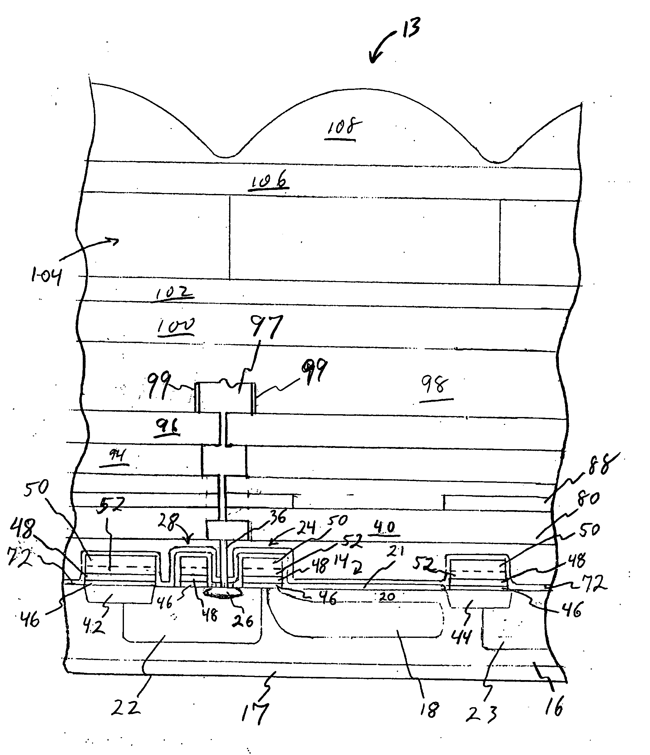
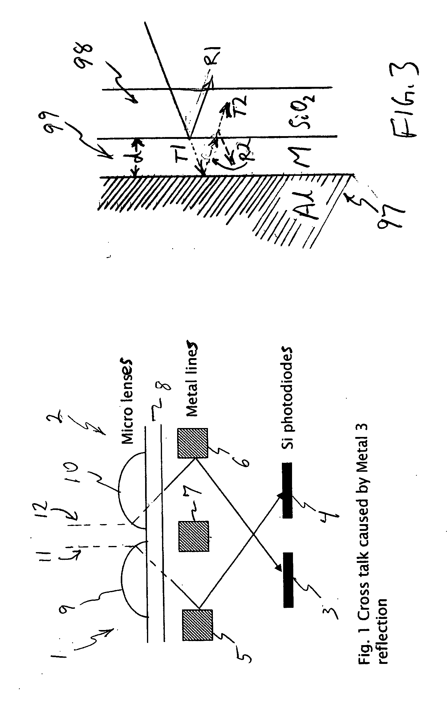
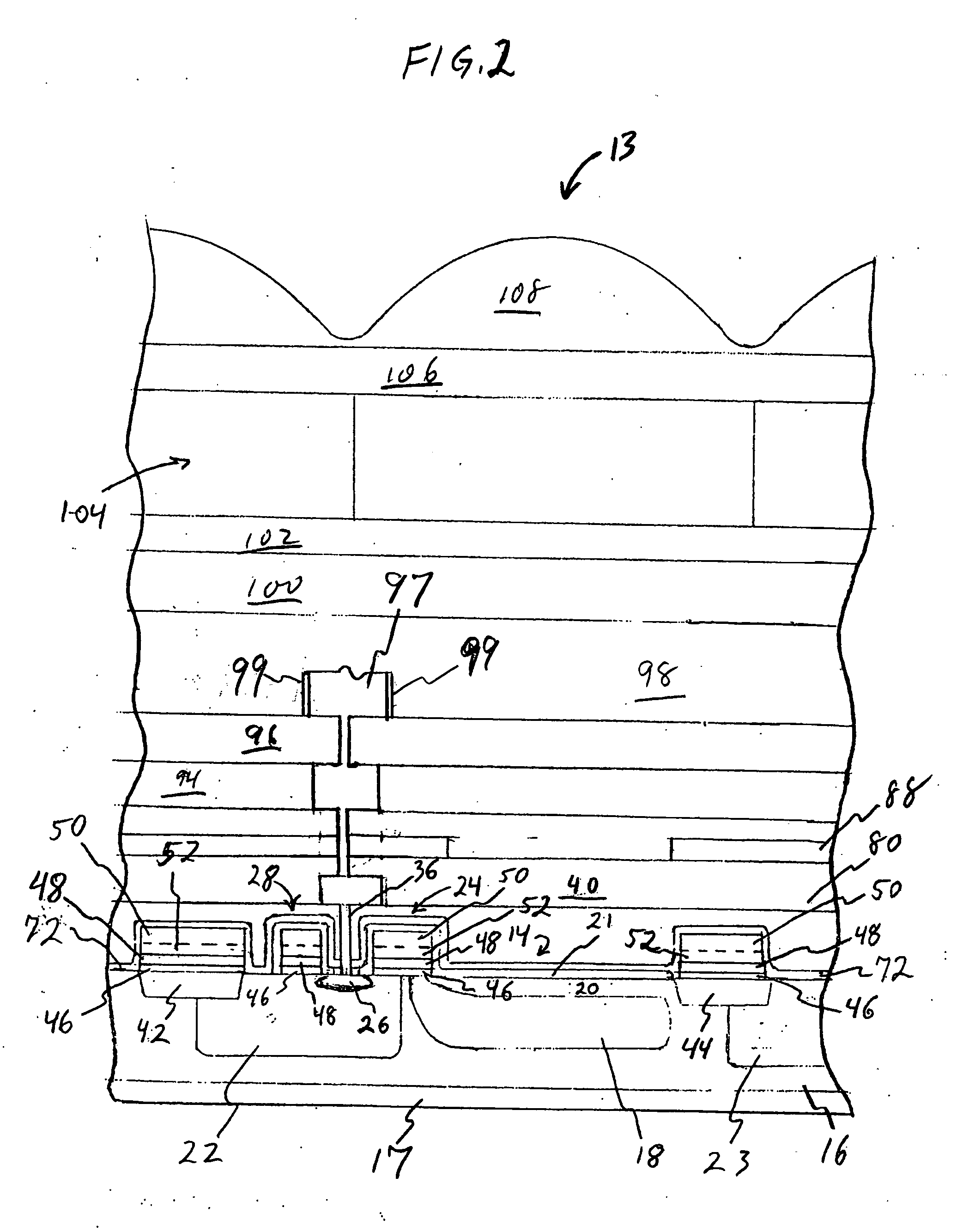
[0029] In the following detailed description, reference is made to the accompanying drawings which form a part hereof and illustrate specific exemplary embodiments by which the invention may be practiced. It should be understood that like reference numerals represent like elements throughout the drawings. These embodiments are described in sufficient detail to enable those skilled in the art to practice the invention. It is to be understood that other embodiments may be utilized, and that structural, logical, and electrical changes may be made without departing from the spirit and scope of the invention.

[0030] The term “substrate” is to be understood as including silicon, silicon-on-insulator (SOI), or silicon-on-sapphire (SOS) technology, doped and undoped semiconductors, epitaxial layers of silicon supported by a base semiconductor foundation, and other semiconductor structures. Furthermore, when reference is made to a “substrate” in the following description, previous process st...


PUM


Abstract

Conductive lines in an imaging device are coated with an anti-reflective film to reduce crosstalk caused by light reflecting from the conductive lines. An interface results between the anti-reflective film and the surface of the conductive line surface. A second interface exists between the anti-reflective film and an overlying insulating layer. The anti-reflective film is formed from a material having a complex refractive index such that reflectance is reduced at each of the two interfaces. The anti-reflective film also can be light absorbing to provide further reductions in light reflection and consequent crosstalk.

Description

BACKGROUND OF THE INVENTION [0001] 1. Field of the Invention [0002] The invention relates generally to semiconductor imaging devices and in particular to a semiconductor-based imaging device having structures for reducing optical crosstalk among pixels. [0003] 2. Discussion of Related Art [0004] Semiconductor imaging devices include charge coupled devices (CCDs), photodiode arrays, charge injection devices, and hybrid focal plane arrays. CCDs are often employed for image acquisition and enjoy a number of advantages which makes it the incumbent technology, particularly for small-size imaging applications. CCDs are also capable of large formats with small pixel-size and they employ low-noise charge-domain processing techniques. [0005] Inherent limitations in CCD technology have promoted interest in CMOS imagers for possible use as a low-cost imaging-device alternative. Advantages of CMOS imagers over CCD imagers include low-voltage operation and low power-consumption. Also, CMOS image...

Claims


Application Information

Patent Timeline
Patent Type & Authority Applications(United States)
IPC IPC(8): H01L33/00
CPCH01L27/14609H01L27/1462H01L27/14636H01L27/14627H01L27/14623H01L27/146H04N25/62
Inventor LI, JIUTAO
Owner MICRON TECH INC
Why Eureka
Try Eureka