
Interferometric measuring device and projection exposure installation comprising such measuring device

a technology of interferometry and measuring devices, which is applied in the direction of photomechanical devices, instruments, printers, etc., can solve problems such as the optical properties of the device, and achieve the effect of simple structure, rapid and fault-free measurements

Inactive Publication Date: 2007-03-01
CARL ZEISS SMT GMBH
View PDF27 Cites 3 Cited by
  • Summary
  • Abstract
  • Description
  • Claims
  • Application Information

AI Technical Summary

Benefits of technology

This solution enables rapid and fault-free measurements of projection objectives during operation, reducing machine downtimes and increasing productivity by integrating the measurement structures directly into the reticle used for chip production, allowing for timely detection and correction of imaging quality issues.

Problems solved by technology

Since, on account of the complicated optical structure, it is as a rule impossible to derive the optical properties of the objectives from theoretical calculations, the optical properties have to be measured reliably, at least during the assembly and the adjustment of the optical imaging systems.

Method used


Image

  • Interferometric measuring device and projection exposure installation comprising such measuring device
  • Interferometric measuring device and projection exposure installation comprising such measuring device
  • Interferometric measuring device and projection exposure installation comprising such measuring device

Examples


Embodiment Construction

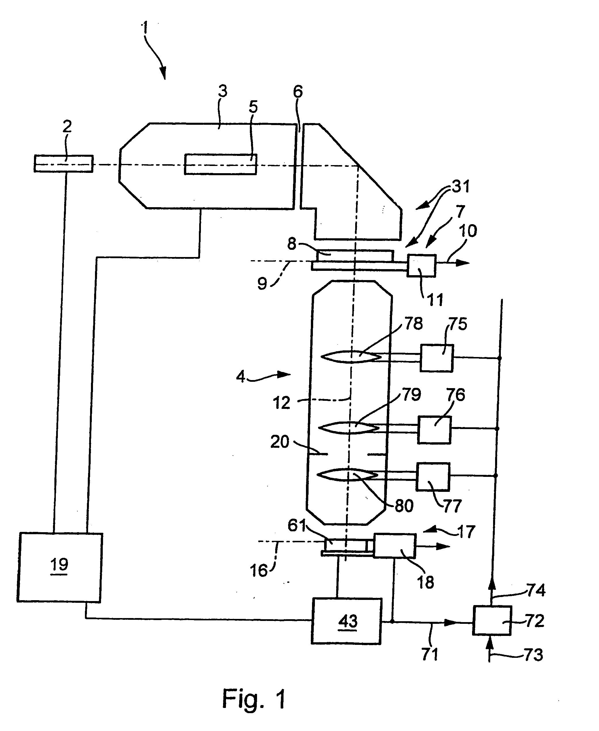
[0038]FIG. 1 shows in schematic form a microlithography projection exposure installation in the form of a wafer stepper 1, which is provided for the production of highly integrated semiconductor components. The projection exposure installation comprises an excimer laser 2 as the light source, which emits light with an operating wavelength of 248 nm, it being possible for the operating wavelength in other embodiments also to lie below this, for example at 193 nm or 157 nm, or above this. There are also systems which operate with shorter wavelengths from the EUV range and corresponding light sources. An illumination system 3 connected downstream generates a large, sharply delimited and homogeneously illuminated image field, which is adapted to the telecentric requirements of the projection objective 4 connected downstream. The projection objective 4 is a preferred embodiment of an optical imaging system to be measured. The illumination system has devices for selecting the illuminating...


PUM

PropertyMeasurementUnit
anglesaaaaaaaaaa
anglesaaaaaaaaaa
anglesaaaaaaaaaa

Abstract

A measuring device for interferometric measurement of an optical imaging system that is provided for projecting a useful pattern, provided on a mask, into the image plane of the imaging system, includes a wavefront source for generating at least one wavefront traversing the imaging system; a diffraction grating, arrangeable downstream of the imaging system, for interacting with the wavefront reshaped by the imaging system; and a spatially resolving detector, assigned to the diffraction grating, for acquiring interferometric information. The wavefront source has at least one measuring pattern that is formed on the mask in addition to the useful pattern. The useful pattern may represent the structure of a layer of a semiconductor component in a specific fabrication step. The measuring pattern may be formed as a coherence-forming structure periodic in one or two dimensions.

Description

[0001] This application is a divisional of application Ser. No. 10 / 964,868 filed Oct. 15, 2004, the entire disclosure of which is incorporated herein by reference. Priority is claimed from German Patent Application 102 17 242.0 filed Apr. 15, 2002. The disclosure of International Application PCT / EP03 / 03566 is incorporated herein by reference.BACKGROUND OF THE INVENTION [0002] 1. Field of the Invention [0003] The invention relates to a measuring device for interferometric measurement of an optical imaging system and to a microlithographic projection exposure installation in which such a measuring device is integrated. [0004] 2. Discussion of the Related Art [0005] Higher and higher requirements are being placed on the imaging quality of optical imaging systems. One example of this is projection objectives for microlithographic production of semiconductor components and other finely structured components which are intended to produce structures in the sub-micrometer range largely free...

Claims


Application Information

Patent Timeline
Patent Type & Authority Applications(United States)
IPC IPC(8): G03B27/52G02B5/02G01B9/02G03F1/08G03F7/20H01L21/027
CPCG02B5/0221G03F7/706G03F7/70075G02B5/0252
Inventor SCHRIEVER, MARTINWEGMANN, ULRICHHAIDNER, HELMUT
Owner CARL ZEISS SMT GMBH
Learn More