Method of manufacturing silicon wafer

a manufacturing method and technology of silicon wafer, applied in the direction of crystal growth process, polycrystalline material growth, after-treatment details, etc., can solve the problems of high cost, excessive point defects, and poor productivity of wafers, so as to improve the productivity of wafer manufacturing, the effect of reducing the number of defects

Active Publication Date: 2007-03-15
GLOBALWAFERS JAPAN
View PDF10 Cites 21 Cited by
  • Summary
  • Abstract
  • Description
  • Claims
  • Application Information

AI Technical Summary

Benefits of technology

[0025] Further, in the manufacture method of the silicon wafer in accordance with the present invention, an example of the above-mentioned single crystal ingot to be used may be one that is grown under growth conditions where a pulling speed is high and a void-like defect takes place. As a result, it is possible to considerably improve the productivity of wafer manufacture.
[0026] As described above, according to the present invention, the wafer surface layer part on which the device is formed has considerably few minute defects, such as LSTD (Laser scattering tomography defect), and it is possible to manufacture a silicon wafer sufficiently available for next generation and next generation LSI's and an individual semiconductor device, etc. with sufficient productivity at low cost.

Problems solved by technology

Such a void type defect existing in the surface layer part of the silicon wafer damages an oxide film withstand voltage characteristic and may be a reason for adversely affecting an electrical property of the semiconductor device formed at the wafer.
However, there is a problem in that such a wafer has poor productivity and is very costly.
In addition, when the wafer is heated to a high temperature in such an RTA process, inter-lattice silicon (Si) and point defects of cavities take place inside the wafer at a high concentration.
Then, rapid quench (cooling) of the wafer causes the point defects to be excessive and diffuse outwards to the wafer surface.
However, when the rise speed in temperature is equal to or less than 150° C. / sec within the above-mentioned range of the heat treatment temperature, the inter-lattice Si out of the inter-lattice silicon (Si) and the cavity generated due to the rising temperature is emitted towards the wafer surface by diffusion., Thus, the grown-in defect on the above-mentioned surface of the wafer is removed, but the grown-in defect existing inside the wafer surface layer cannot be removed, which results in a disadvantage that the grown-in defect remains in a device activity layer of the wafer surface layer part.

Method used


Image

  • Method of manufacturing silicon wafer
  • Method of manufacturing silicon wafer
  • Method of manufacturing silicon wafer

Examples


example 1

[0050] As a silicon (Si) wafer, one that was a substrate obtained by Czochralski method (CZ), of P-type (boron doped), having a diameter of 300 mm, a direction (100), electric resistivity of 1-10 Ωcm, and an initial oxygen concentration of 10×1017 atoms / cm3 was prepared.

[0051] Then, this substrate was subjected to LSA processing (temperature: 1300° C., period of time: 0.01 microseconds-50 milliseconds).

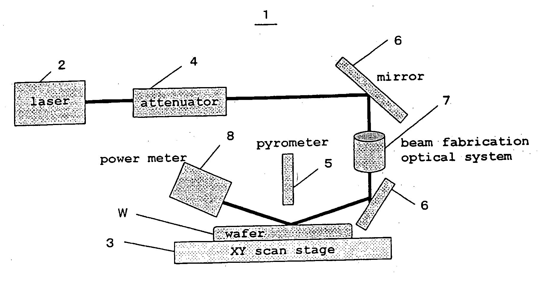
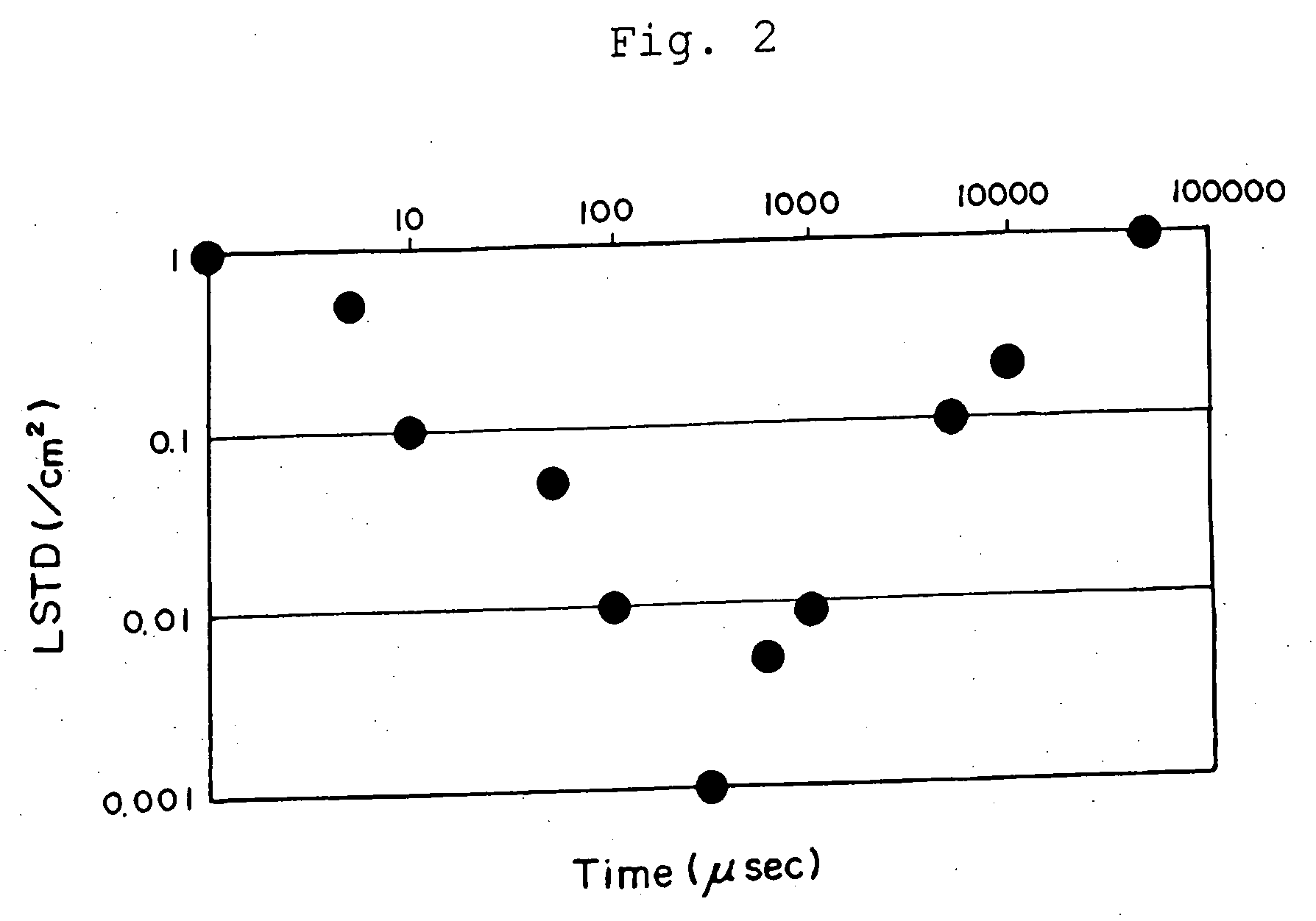
[0052] In addition, a diameter of an irradiation beam was 1 mm, and the entire surface of the wafer having a diameter of 300 mm was subjected to the LSA processing for about 5 minutes. The result is shown in FIG. 1. In addition, a relationship between an LSA period (microsecond) and LSTD (Laser scattering tomography defect) ( / cm2) is shown in FIG. 2.

[0053] As shown in FIG. 2, according to the present invention, LSTD may be 0.1 / cm2 or less by way of LSA processing where laser irradiation period is 10 microseconds-0.8 milliseconds.

[0054] As described above, the manufacture method of...


PUM

PropertyMeasurementUnit
temperatureaaaaaaaaaa

Abstract

The present invention provides a method of manufacturing a silicon wafer where a defect does not exist at a wafer surface layer part on which a device is formed, without affecting productivity and production costs of the wafer. An ingot of a silicon single crystal is grown by way of Czochralski single crystal pulling method, this silicon single crystal ingot is sliced to produce a wafer, then a surface layer of the wafer is annealed for between 0.01 microseconds and 10 seconds (inclusive) by means of a laser spike annealing apparatus such that a temperature of a wafer surface layer part is between 1250° C. and 1400° C. (inclusive).

Description

CROSS-REFERENCE TO RELATED PATENT APPLICATIONS [0001] The right of foreign priority is claimed under 35 U.S.C. § 119(a) based on Japan Application No. 2005-263417, filed Sep. 12, 2005, the entire contents of which, including the specification, drawings, claims and abstract, are incorporated herein by reference. BACKGROUND OF THE INVENTION [0002] 1. Field of the Invention [0003] The present invention relates to a method of manufacturing a silicon wafer and a silicon wafer, in particular to a method of manufacturing a silicon wafer using a laser spike anneal process. [0004] 2. Description of the Related Art [0005] It is important for a surface layer part of a silicon wafer for manufacturing a device to have substantially no defects in order to improve electrical characteristics of the wafer, especially an oxide film withstand voltage characteristic. [0006] Usually, in most cases, a void type defect (also referred to as a grown-in defect) referred to as COP (Crystal Originated Particle...

Claims


Application Information

Patent Timeline
Patent Type & Authority Applications(United States)
IPC IPC(8): H01L21/20
CPCC30B15/00C30B29/06H01L21/3221H01L21/2026H01L21/268C30B33/02Y10S117/904Y10S438/974H01L21/02667H01L21/02532
Inventor IZUMOME, KOJI
Owner GLOBALWAFERS JAPAN
Why Eureka
Try Eureka