Photomask, method for fabricating photomask, and method for fabricating semiconductor device

a technology of photomask and semiconductor, which is applied in the direction of photomechanical equipment, originals for photomechanical treatment, instruments, etc., can solve the problems of stray light still adversely affecting the transfer of circuit patterns to wafers, the accuracy of line width in such transfer patterns is greatly affected, and the manufacturing cost of photomasks for forming patterns increases. , to achieve the effect of suppressing the effect of stray light, high positional accuracy and high accuracy patterning

Inactive Publication Date: 2007-03-22
FUJITSU SEMICON LTD
View PDF3 Cites 15 Cited by
  • Summary
  • Abstract
  • Description
  • Claims
  • Application Information

AI Technical Summary

Benefits of technology

[0035] The inventor proposes a photomask which can achieve high patterning accuracy of a circuit pattern transferred to a wafer and can suppress the effect of stray light without drastically increasing cost.
[0036] In order to overcome the problems described above, the inventor has found that a phase shift layer, which is used for enhancing contrast of a circuit pattern, can be used for absorbing stray light. In such a case, by devising a method for fabrication as described below, it is possible to fabricate a high-accuracy photomask while suppressing an increase in cost. Thus, the present invention has been achieved.
[0040] Furthermore, because of the light absorbing effect of the phase shift layer (light-absorbing pattern) remaining in the peripheral region, the phase shift layer absorbs stray light, and the amount of stray light is greatly decreased. As a result, when a circuit pattern is formed by patterning on the wafer, the influence of stray light is suppressed.
[0044] In accordance with the present invention, with respect to a photomask used for projection exposure, it is possible to suppress the effect of stray light without drastically increasing cost while achieving high patterning accuracy of a circuit pattern transferred to a wafer.

Problems solved by technology

Hence, stray light still adversely affects the transfer of a circuit pattern to a wafer.
As the pattern formed on a semiconductor chip becomes finer, manufacturing cost of the photomask for forming the pattern increases.
Consequently, the accuracy of line width in such a transfer pattern is greatly affected by the positional accuracy of irradiation of the electron beam in addition to the energy profile of the electron beam.
Additionally, when patterning is performed by type (B) photolithography, described above (i.e. if a negative photoresist with high patterning accuracy is used), a long period of time is required for exposure.
This extended time results in an increase in manufacturing cost.
Also, strain tends to occur in the photomask due to prolonged heat exposure.
Therefore, the related art does not achieve both reduction in manufacturing cost and high-precision patterning.

Method used


Image

  • Photomask, method for fabricating photomask, and method for fabricating semiconductor device
  • Photomask, method for fabricating photomask, and method for fabricating semiconductor device
  • Photomask, method for fabricating photomask, and method for fabricating semiconductor device

Examples


example

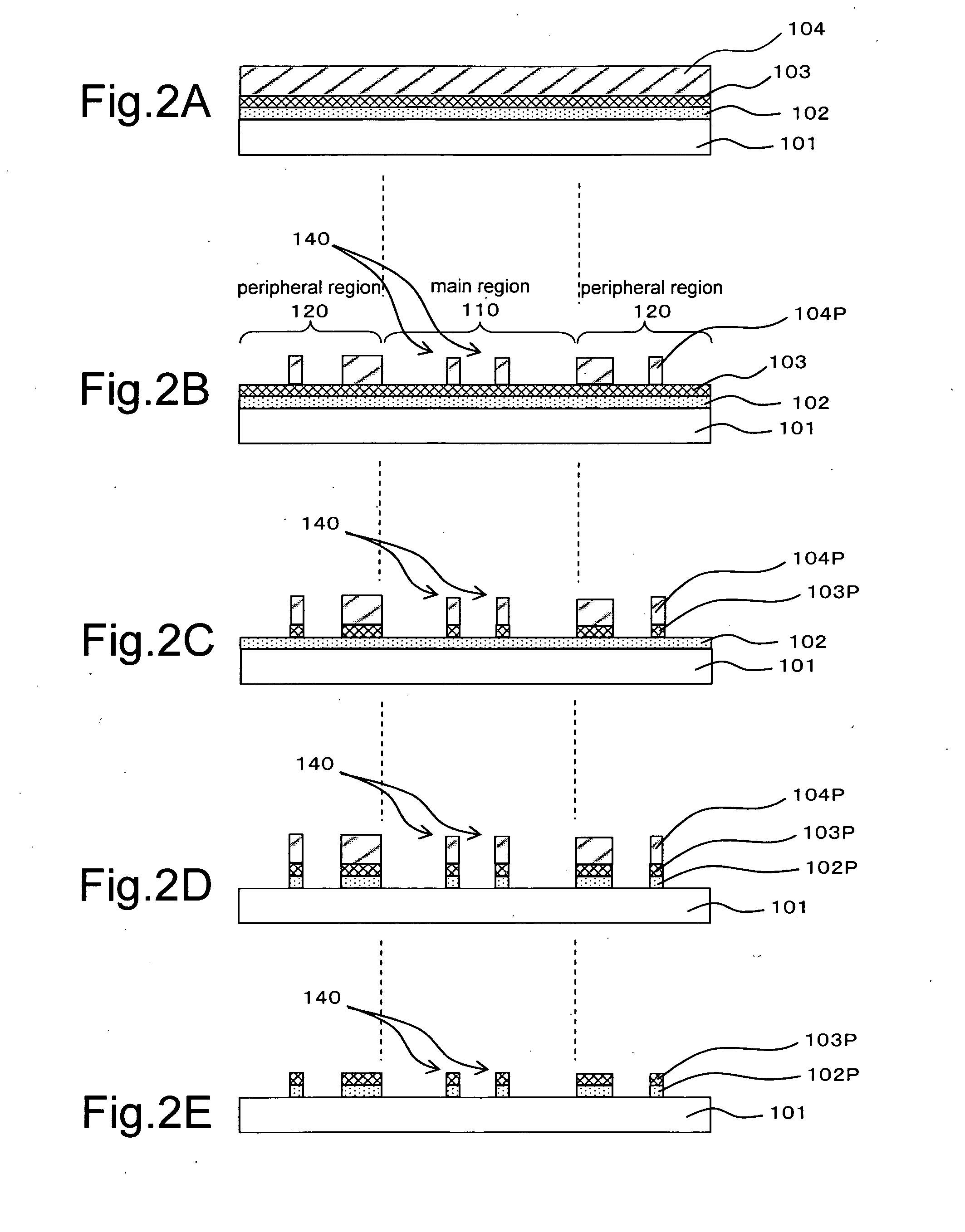
[0077] An example of a method for fabricating a device using a photomask according to the present invention will be described below with reference to FIGS. 7A, 7B, 8C, 8D, 9E, 9F, 10G, and 10H.

[0078] First, in a silicon substrate (wafer) 10, element isolation films 12 embedded in trenches having a depth of, for example, 300 nm are formed, for example, by a shallow trench isolation (STI) process (refer to FIG. 7A). In the drawing, a left-side element region corresponds to an N-type transistor forming region, and a right-side element region corresponds to a P-type transistor forming region.

[0079] Subsequently, for example, using a thermal oxidation method, a sacrificial oxide film 14 is formed over the element regions delimited by the element isolation films 12 (refer to FIG. 7B).

[0080] Then, a first photoresist film 16 is formed by photolithography so as to expose the N-type transistor forming region and cover the P-type transistor forming region (refer to FIG. 8C).

[0081] Using t...


PUM

PropertyMeasurementUnit
transmittanceaaaaaaaaaa
depthaaaaaaaaaa
thicknessaaaaaaaaaa

Abstract

A method for fabricating a photomask includes the steps of forming a phase shift layer, a light-shielding layer, and a negative resist layer in that order on a transparent substrate, forming a first resist pattern including a pattern corresponding to a transfer pattern by performing first exposure and development on the negative resist layer, forming a light-shielding pattern by etching the light-shielding layer using the first resist pattern as a mask, removing the first resist pattern, and then forming a positive resist layer thereon, forming a second resist pattern including a pattern corresponding to a light-absorbing pattern by performing second exposure and development on the positive resist layer, and forming a phase shift pattern by etching the phase shift layer using the second resist pattern as a mask.

Description

BACKGROUND OF THE INVENTION [0001] 1. Field of the Invention [0002] The present invention relates to a photomask mainly used for projection aligners, a method for fabricating a photomask, and a method for fabricating a semiconductor device. More particularly, the invention relates to a photomask having a function of shifting a phase of projected exposure light passing through the photomask, a method for fabricating the photomask, and a method for fabricating a semiconductor device using such a photomask. [0003] 2. Description of the Related Art [0004] Recently, in the fabrication of large-scale integrated circuits (LSIs), formation of very fine patterns are required. Consequently, in the exposure process in which fine circuit patterns are transferred onto semiconductor substrates (hereinafter referred to as “wafers”), photomasks having a function of shifting phases of exposure light to increase contrast (hereinafter referred to as “phase shift masks”) have been used. [0005] Among th...

Claims


Application Information

Patent Timeline
Patent Type & Authority Applications(United States)
IPC IPC(8): G03F1/00G03C5/00G03F1/32G03F1/54G03F7/11G03F7/40
CPCG03F1/14G03F1/42G03F1/38G03F1/32
Inventor ISHIWATA, NAOYUKI
Owner FUJITSU SEMICON LTD
Why Eureka
Try Eureka