Polymeric microarray support, method of forming microfeatures on an optical assay arrangement
- Summary
- Abstract
- Description
- Claims
- Application Information
AI Technical Summary
Benefits of technology
Problems solved by technology
Method used
Image
Examples
first embodiment
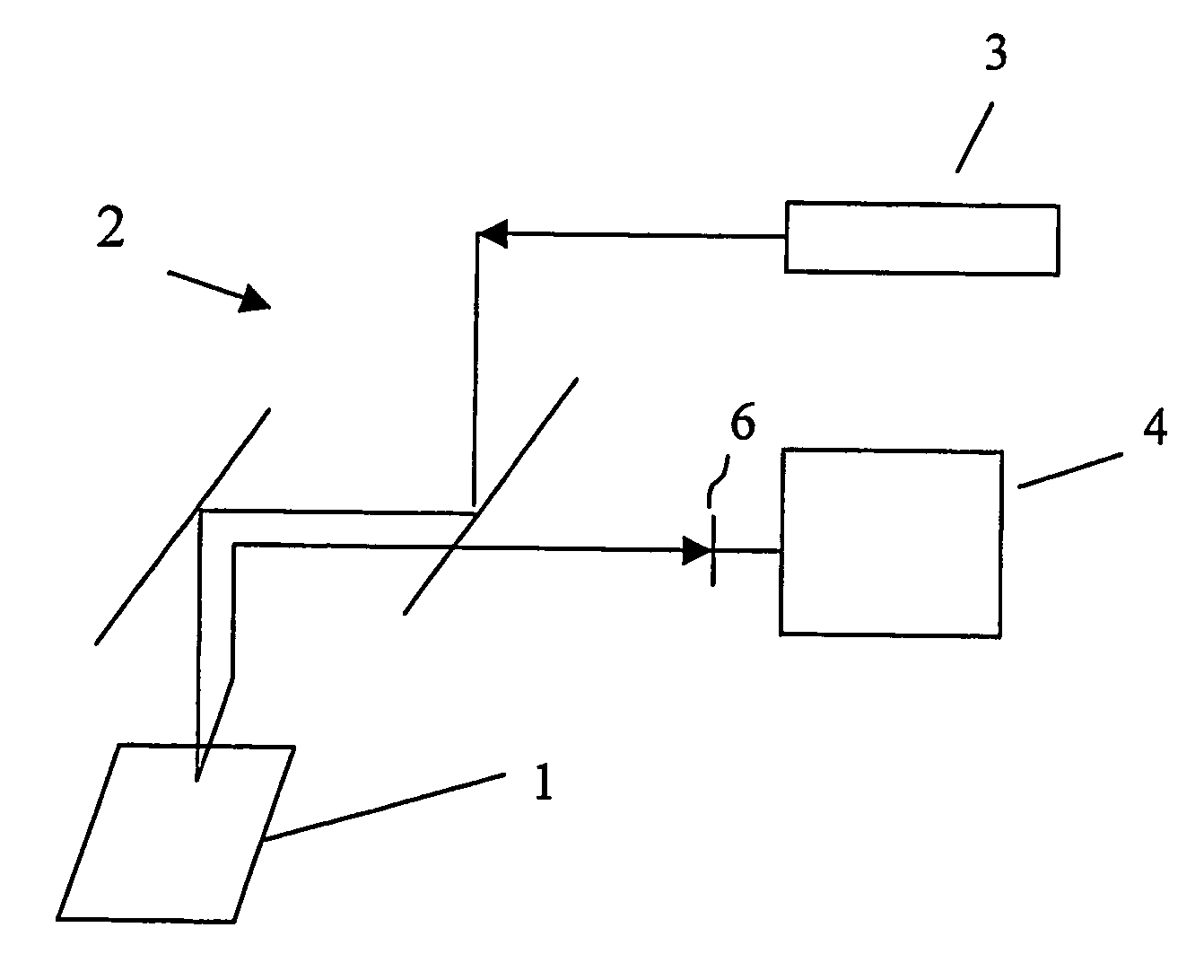
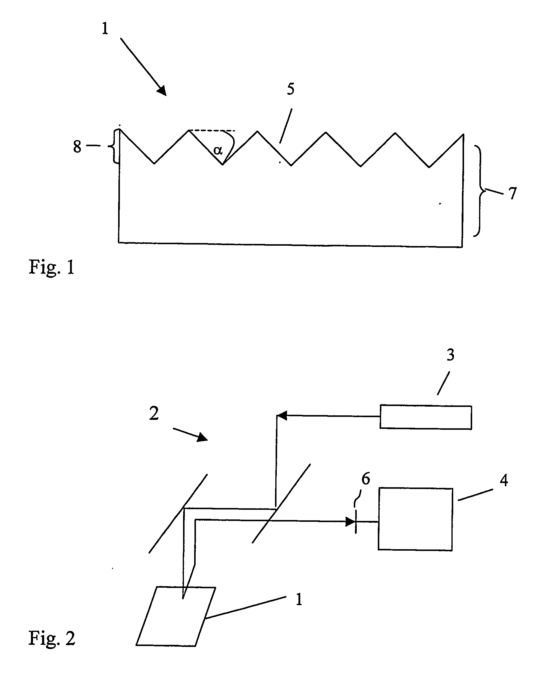
[0040] According to the invention, the microfeatures of the support comprise a surface enlarging pattern, e.g. V-grooves, the depth of the grooves being adapted to the depth of focus of the optical means of the assay arrangement, such that the sum of the selected depth of the grooves and of the variation in the thickness of the support substantially corresponds to the depth of focus.
[0041] In an exemplary embodiment, the grooves are pyramidically-shaped, the grooves master structure being anisotropically etched in (100) silicon, resulting in a tilt angle of 55°. If the depth of focus of the optical means is 20-30 micrometers and the quality of the support slide limits the variations in the support thickness to 10-15 micrometer, the depth of the grooves, may be selected to e.g. 5-10 micrometer. Thereby, the sum of the depth of the grooves and of the thickness variation over the area of the support slide will be 15-25 micrometer. Consequently, the sum will be well within said depth of...
second embodiment
[0047] According to the invention, the performance of the support is further increased by providing a reflecting layer made of a metallic, semiconducting, or a dielectric material. For visible light, a layer of silver, platinum, palladium or gold is beneficial. The thickness of the layer is preferably adapted to the desired transparency of the support, and the layer may be located on the top surface of the support substrate or in the bottom of the support. For example, a 20 nm thick gold film transmits approximately 50% of the red light. One advantage with an additional, metallic layer is that surface chemistry is easier to adopt on a metallic layer than on a polymeric surface. A further advantage is the possibility to use semi-transmitting properties of the layer, i.e. by using the specific wavelength regions of absorption found in metals, semiconductors and dielectrics to make the layer transmit certain wavelengths and reflect other wavelengths.
third embodiment
[0048] According to the invention, the support comprises grooves forming micro-pillars, i.e. cylindrical pillars. According to one exemplary embodiment, the pillars are provided with an additional layer having a larger index of refraction than the support material, thereby achieving an optical waveguide. According to a further exemplary embodiment, particles of suitable size, i.e. typically in the range between 0.1 and 50 micrometers, are located between the micropillars, which improves the signal-to-noise ratio.
PUM
| Property | Measurement | Unit |
|---|---|---|
| Thickness | aaaaa | aaaaa |
| Transparency | aaaaa | aaaaa |
| Distance | aaaaa | aaaaa |
Abstract
Description
Claims
Application Information


