Cobalt silicon contact barrier metal process for high density semiconductor power devices

a technology of copper silicon and contact barrier, which is applied in the direction of semiconductor devices, electrical equipment, basic electric elements, etc., can solve the problems of metal contact with technical difficulties and limitations, yield loss and reliability problems, and the ti/tin metal barrier in trenched mosfet is at the expense of device performan

Inactive Publication Date: 2007-04-05
ALPHA & OMEGA SEMICON LTD
View PDF15 Cites 10 Cited by
  • Summary
  • Abstract
  • Description
  • Claims
  • Application Information

AI Technical Summary

Benefits of technology

[0008] It is therefore an object of the present invention to provide a new and improved semiconductor power device implemented with a cobalt-silicon metal barrier contact to circumvent the problems of dopant loss at the contact interface such that the limitations of the conventional methods can be overcome.
[0009] Specifically, it is an object of the present invention to provide improved MOSFET devices manufactured with a trenched gate by implementing a new and unique CoSi / Ti / TiN metal barrier structure for trenched DMOS. Such device configuration also has a unique process with higher activation temperature window to overcome the bonding related reliability deficiencies and the limitations caused by the DMOS performance degradation as that encountered in the conventional semiconductor power devices.

Problems solved by technology

With bonding wires of larger diameters, conventional techniques for manufacturing a trenched metal oxide semiconductor field effect transistor (MOSFET) implemented either without a metal barrier or with a titanium / titanium nitride (Ti / TiN) barrier for the metal contacts are therefore confronted with technical difficulties and limitations.
Specifically, a high-density trenched semiconductor power device that is implemented without a metal barrier cannot sustain these bonding wires with larger diameters and often leads to yield losses and reliability problems.
Method and devices are also disclosed in U.S. Pat. Nos. 5,693,562 and 5,950,090 to manufacture a semiconductor device implementing a barrier layer composed of Ti / TiN to improve the reliability of the contact metal, However, the implementation of a Ti / TiN metal barrier in a trenched MOSFET is at the expense of device performance.
Such adversely effects to the device performance due the implementation of the Ti / TiN barrier layer for the purpose of improving bonding wire reliability were not considered as significant and mostly unnoticed until recently when the resistance has been significantly reduced due to the shrinking of cell size and increase of number of cell per unit.
However, such process changes are costly and of very limited practical usefulness due to the increase in production costs and additional complexities added to the manufacturing processes.

Method used


Image

  • Cobalt silicon contact barrier metal process for high density semiconductor power devices
  • Cobalt silicon contact barrier metal process for high density semiconductor power devices
  • Cobalt silicon contact barrier metal process for high density semiconductor power devices

Examples


Embodiment Construction

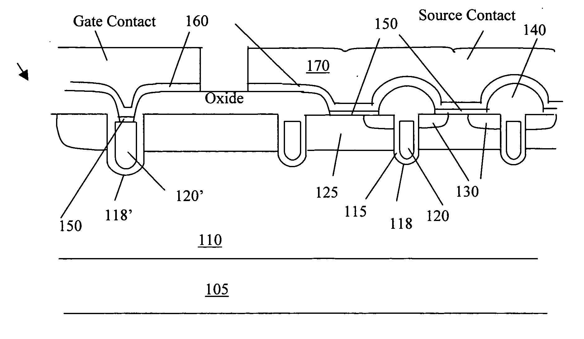
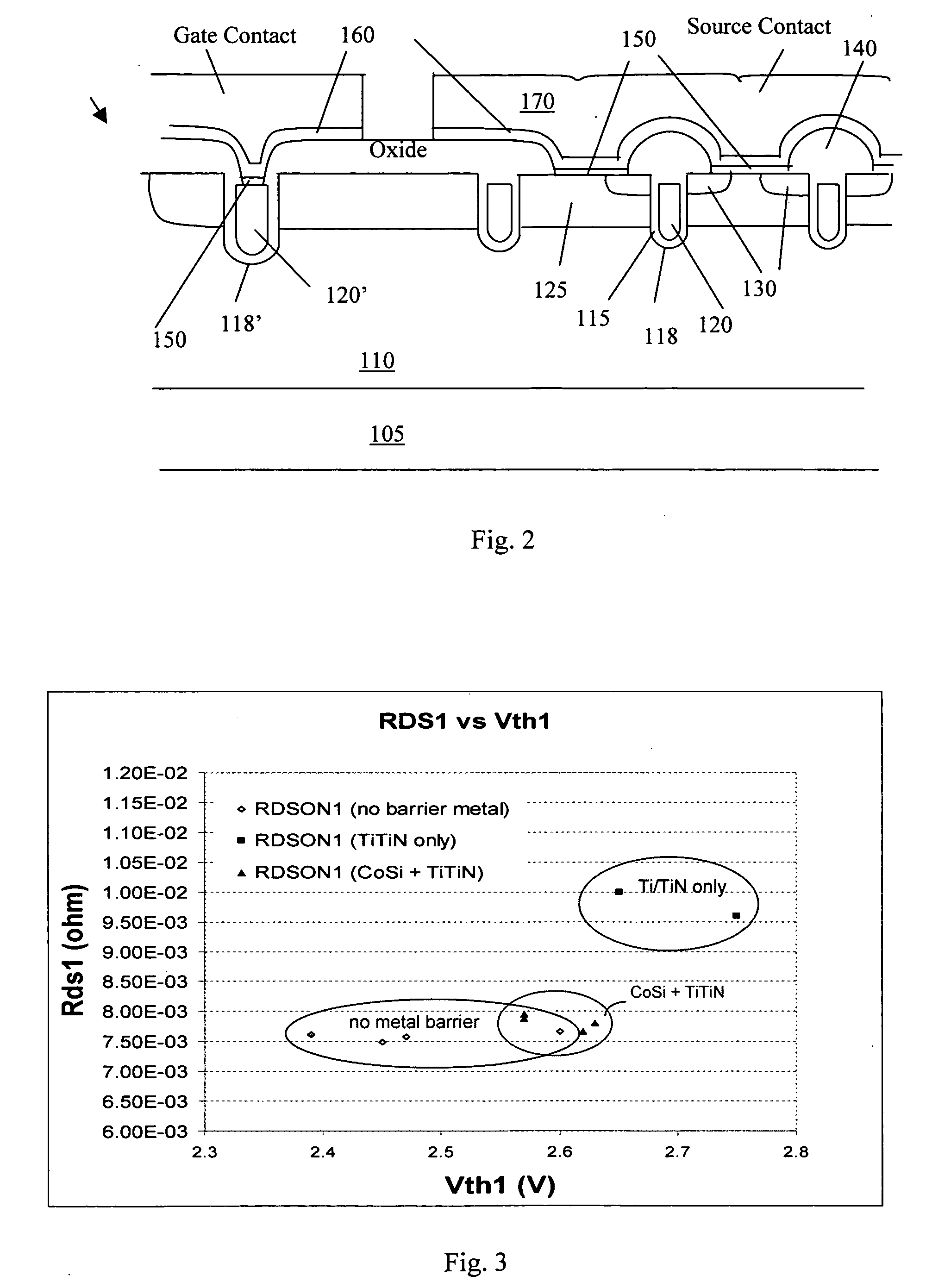
[0016] Referring to FIG. 2 for a cross sectional view of a trenched DMOS device 100. The trenched DMOS device 100 is supported on a substrate 105 formed with an epitaxial layer 110. The trenched DMOS device 100 includes a trenched gate 120 disposed in a trench 118 with a gate insulation layer 115 formed over the walls of the trench. A body region 125 that is doped with a dopant of second conductivity type, e.g., P-type dopant, extends between the trenched gates 120. The P-body regions 125 encompassing a source region 130 doped with the dopant of first conductivity, e.g., N+ dopant. The source regions 130 are formed near the top surface of the epitaxial layer surrounding the trenched gates 120. The top surface of the semiconductor substrate extending over the top of the trenched gate, the P body regions 125 and the source regions 130 are covered with a dielectric protective layers 140. The trenched DMOS device 100 also includes an insulated gate runner 120′ disposed in a gate runner ...


PUM


Abstract

This invention discloses an improved trenched metal oxide semiconductor field effect transistor (MOSFET) cell that includes a trenched gate surrounded by a source region encompassed in a body region above a drain region disposed on a bottom surface of a substrate. The MOSFET cell further includes a source contact opening opened on top of an area extended over the body region and the source region through a protective insulation layer wherein the area further has a cobalt-silicide layer disposed near a top surface of the substrate. The MOSFET cell further includes a Ti / TiN conductive layer covering the area interfacing with the cobalt-silicide layer over the source contact opening. The MOSFET cell further includes a source contact metal layer formed on top of the Ti / TiN conductive layer ready to form source-bonding wires thereon.

Description

BACKGROUND OF THE INVENTION [0001] 1. Field of the Invention [0002] The invention relates generally to the semiconductor power devices. More particularly, this invention relates to an improved and novel contact barrier metal process to manufacture the high-density semiconductor power devices with improved source contact resistance by improving the source contact interfacial layer structures. [0003] 2. Description of the Prior Art [0004] With the advent of high efficiency metal oxide semiconductor (MOS) gate devices for hand held electronics power-switching applications leads to a more stringent requirement to further reduce the on-resistance of the MOSFET device. In order to satisfy this requirement, bonding wires of larger diameter to improve the connection between the semiconductor chip and the external leads. With bonding wires of larger diameters, conventional techniques for manufacturing a trenched metal oxide semiconductor field effect transistor (MOSFET) implemented either wi...

Claims


Application Information

Patent Timeline
Patent Type & Authority Applications(United States)
IPC IPC(8): H01L29/78H01L21/336
CPCH01L21/28518H01L21/76843H01L21/76855H01L29/456H01L29/4933H01L29/4941H01L29/66734H01L29/7811H01L29/7813
Inventor CHANG, HONGLI, TIESHENGTAI, SUNG-SHANNG, DANIELBHALLA, ANUP
Owner ALPHA & OMEGA SEMICON LTD
Why Eureka
Try Eureka