Method for manufacturing compound semiconductor substrate

a technology of semiconductor substrates and semiconductors, applied in the direction of semiconductor devices, basic electric elements, electrical appliances, etc., can solve problems such as deterioration in the performance of electronic devices, and achieve excellent heat radiation, excellent rectification properties, and high current amplification factors

Inactive Publication Date: 2007-04-12
SUMITOMO CHEM CO LTD
View PDF8 Cites 12 Cited by
  • Summary
  • Abstract
  • Description
  • Claims
  • Application Information

AI Technical Summary

Benefits of technology

[0015] The compound semiconductor substrate obtained by the method according to the present invention is excellent in heat radiation. The compound semiconductor substrate is used as a material for manufacturing to obtain electronic devices such as transistor and heterojunction bipolar transistor having a high current amplification factor, and diode of excellent rectification property. These electronic devices are excellent in terms of performances and reliability, since temperature elevation of their devices is reduced even when operated at a high current density.

Problems solved by technology

It is known that, when these electronic devices are operated at a high current density, temperature of the electronic devices rises to result in deterioration in performances of the electronic devices such as current amplification factor of transistor and rectification property of diode and degradation in reliability.

Method used


Image

  • Method for manufacturing compound semiconductor substrate
  • Method for manufacturing compound semiconductor substrate
  • Method for manufacturing compound semiconductor substrate

Examples


example 1

PS [Manufacturing of Compound Semiconductor Substrate]

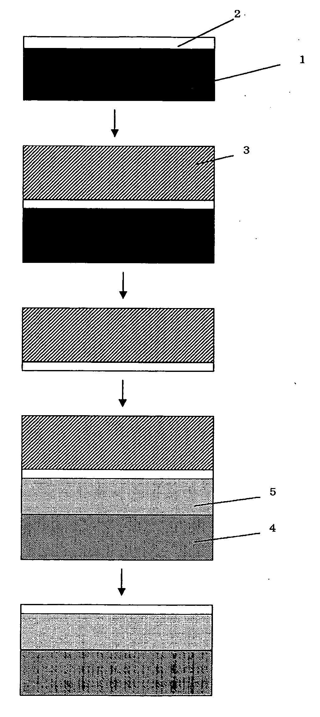
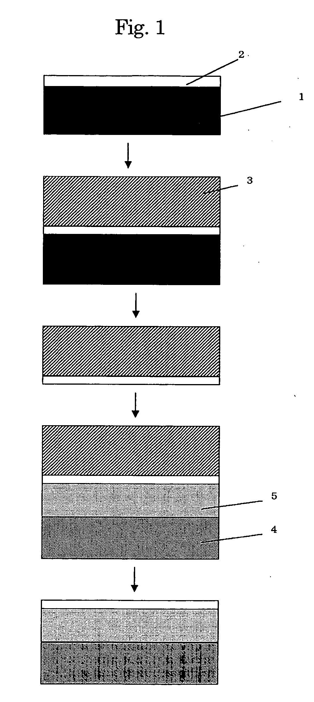
[0047]FIG. 1 shows a procedure for manufacturing a compound semiconductor.

[0048] On a single crystal semi-insulating GaAs substrate 1 having a diameter of 100 mm and a thickness of 630 μm which is commercially available, a compound semiconductor functional layer 2 for a heterojunction bipolar transistor was grown by metal organic vapor-phase thermal decomposition using hydrogen gas as a carrier,

trimethyl gallium, triethyl gallium, trimethyl aluminum, and trimethyl indium as a starting material containing III group element;

arsine and phosphine as a starting material containing V group element; and

disilane (n-type control) and trichloro-bromomethane (p-type control) as a raw material of a dopant for conductivity control, to produce a compound semiconductor layer substrate.

[0049] A layer structure of the compound semiconductor functional layer 2 was described in order from the substrate 1 side, as follows:

undoped GaAs laye...

example 2

[Manufacturing of Compound Semiconductor Substrate]

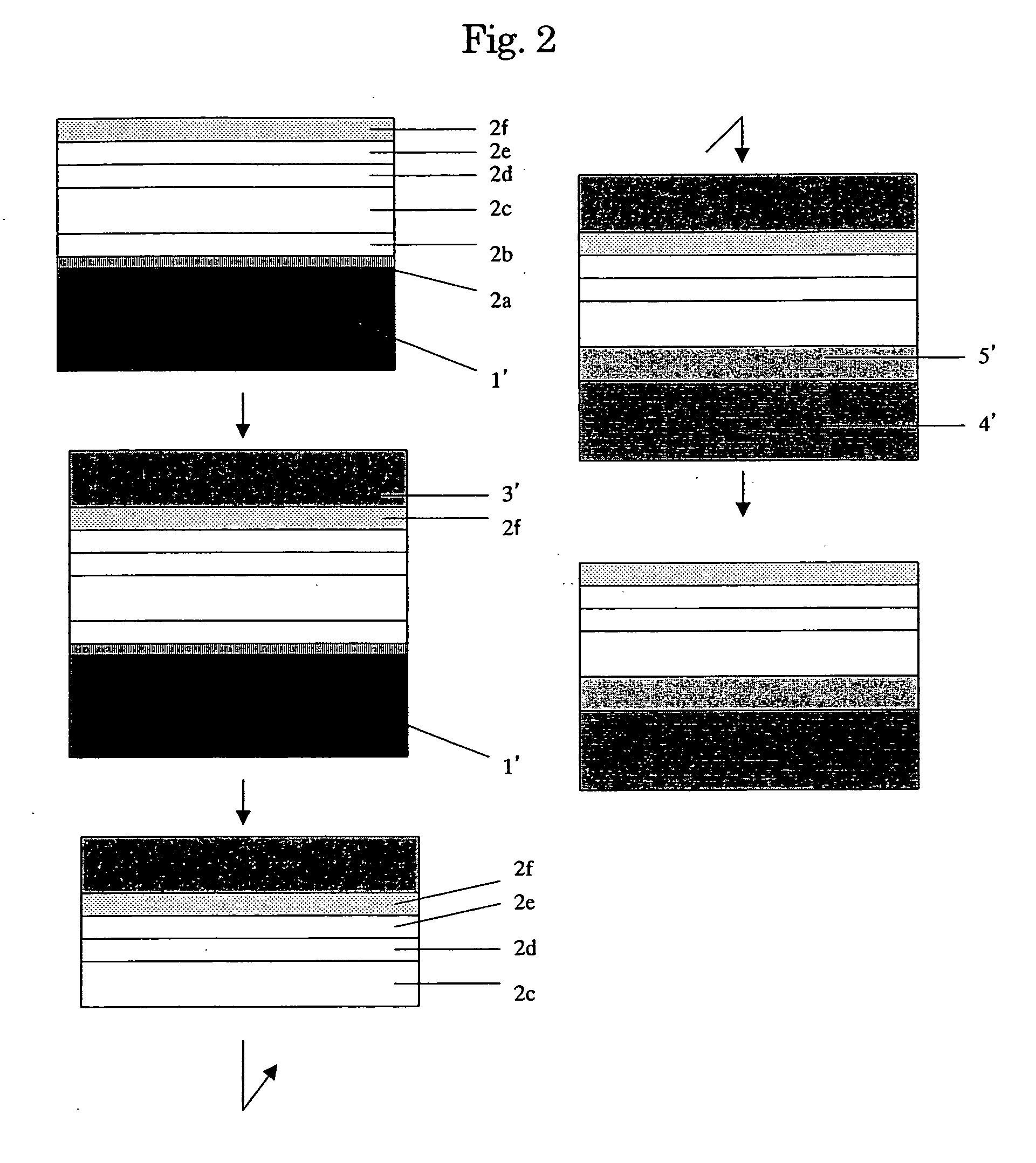
[0056] On a single crystal insulating sapphire substrate 1′ having a diameter of 50 mm and a thickness of 500 μm which is commercially available, a compound semiconductor functional layer 2′ for a pn junction diode was grown by metal organic vapor-phase thermal decomposition using

hydrogen gas as a carrier,

trimethyl gallium, and trimethyl aluminum as a starting material containing III group element; ammonia as a starting material containing V group element; and

silane (n-type control) and bis(cyclopentadienyl)magnesium (p-type control) as a raw material of a dopant for conductivity control to produce a compound semiconductor layer substrate.

[0057] A layer structure of the compound semiconductor functional layer 2′ was described in order from the substrate 1′ side as follows (see FIG. 2):

undoped GaN buffer layer 2a20 nmundoped GaN layer 2b500 nm Si-doped (electron density 3 × 10¹⁸ / cm3)5000 nm n-type GaN layer 2cundoped GaN la...


PUM

PropertyMeasurementUnit
thicknessaaaaaaaaaa
thicknessaaaaaaaaaa
thicknessaaaaaaaaaa

Abstract

The present invention provides a method for manufacturing a compound semiconductor substrate. The method for manufacturing a compound semiconductor substrate comprises the steps of:
  • (a) epitaxially growing a compound semiconductor functional layer 2 on a substrate 1,
  • (b) bonding a support substrate 3 to the compound semiconductor functional layer 2,
  • (c) polishing the substrate 1 and a part of the compound semiconductor functional layer 2 on the side which is in contact with the substrate 1, to remove them,
  • (d) bonding a thermally conductive substrate 4 having a thermal conductivity higher than that of the substrate 1 to the exposed surface of the compound semiconductor functional layer 2 which is provided in the step (c) to obtain a multilayer substrate and
  • (d) separating the support substrate 3 from the multilayer substrate.

Description

TECHNICAL FIELD [0001] The present invention relates to a method for manufacturing a compound semiconductor substrate. BACKGROUND OF THE ART [0002] A compound semiconductor substrate has been used for manufacturing electronic devices such as field-effect transistor, heterojunction bipolar transistor, etc. It is known that, when these electronic devices are operated at a high current density, temperature of the electronic devices rises to result in deterioration in performances of the electronic devices such as current amplification factor of transistor and rectification property of diode and degradation in reliability. In order to reduce temperature elevation of the electronic devices, a method for manufacturing the compound semiconductor substrate which is excellent in heat radiation has been studied. DISCLOSURE OF THE INVENTION [0003] The object of the invention is to provide a method for manufacturing a compound semiconductor substrate which is excellent in heat radiation. [0004]...

Claims


Application Information

Patent Timeline
Patent Type & Authority Applications(United States)
IPC IPC(8): H01L21/20H01L21/36H01L31/20H01L21/30H01L21/46H01L21/335H01L21/331H01L29/20H01L29/737
CPCH01L21/2007H01L29/2003H01L29/66462H01L21/185H01L21/02H01L21/18H01L21/20
Inventor HATA, MASAHIKOONO, YOSHINOBUUEDA, KAZUMASA
Owner SUMITOMO CHEM CO LTD
Why Eureka
Try Eureka