Faceted structure, article, sensor device, and method
- Summary
- Abstract
- Description
- Claims
- Application Information
AI Technical Summary
Benefits of technology
Problems solved by technology
Method used
Image
Examples
example 1
Article Fabrication
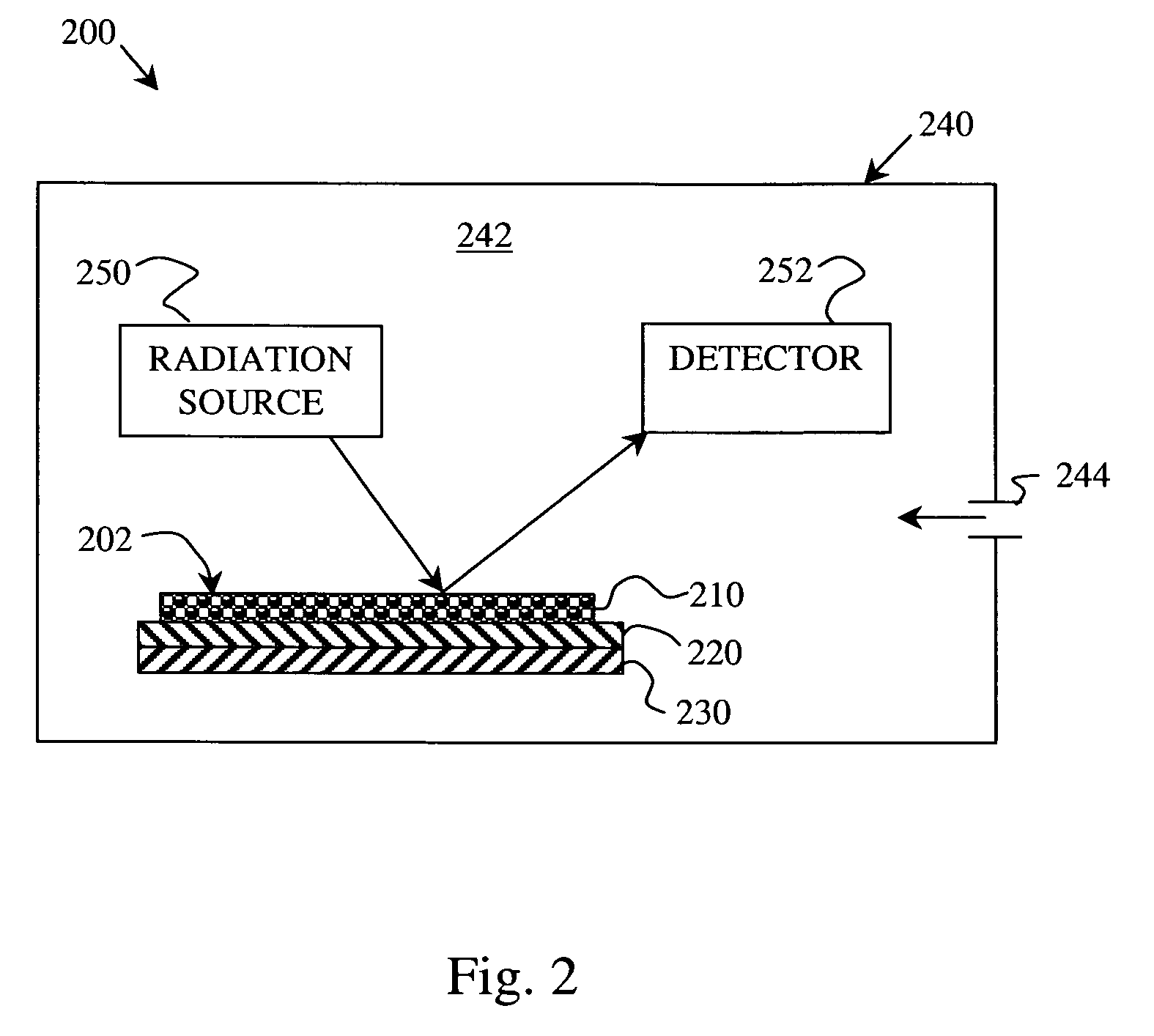
[0137] An article is fabricated by disposing a plurality of faceted structures onto an anode of a scanning electron microscope (SEM). A microscope cathode (radiation source) provides a source of electrons to pump the medium of the device. The plurality of faceted structures define a 1 millimeter by 1 millimeter planar array of gallium-containing nitride crystalline compositions epitaxially grown on an aluminum nitride template layer disposed on a sapphire substrate. The faceted structures are hexagonal prisms or pyramids, each having a nominal base size of about 700 nanometers. The array has a pitch, or a nominal intercrystalline spacing, of about 700 nanometers. Each faceted structure is electrically connected to a grounded anode plate by a copper conductor. A fiber optic probe connects to a spectrometer and monitors emission from the faceted structure as electrons from the SEM cathode impinged upon the faceted structure. Accelerating voltage of the SEM controls...
example 2
Sensor Layers
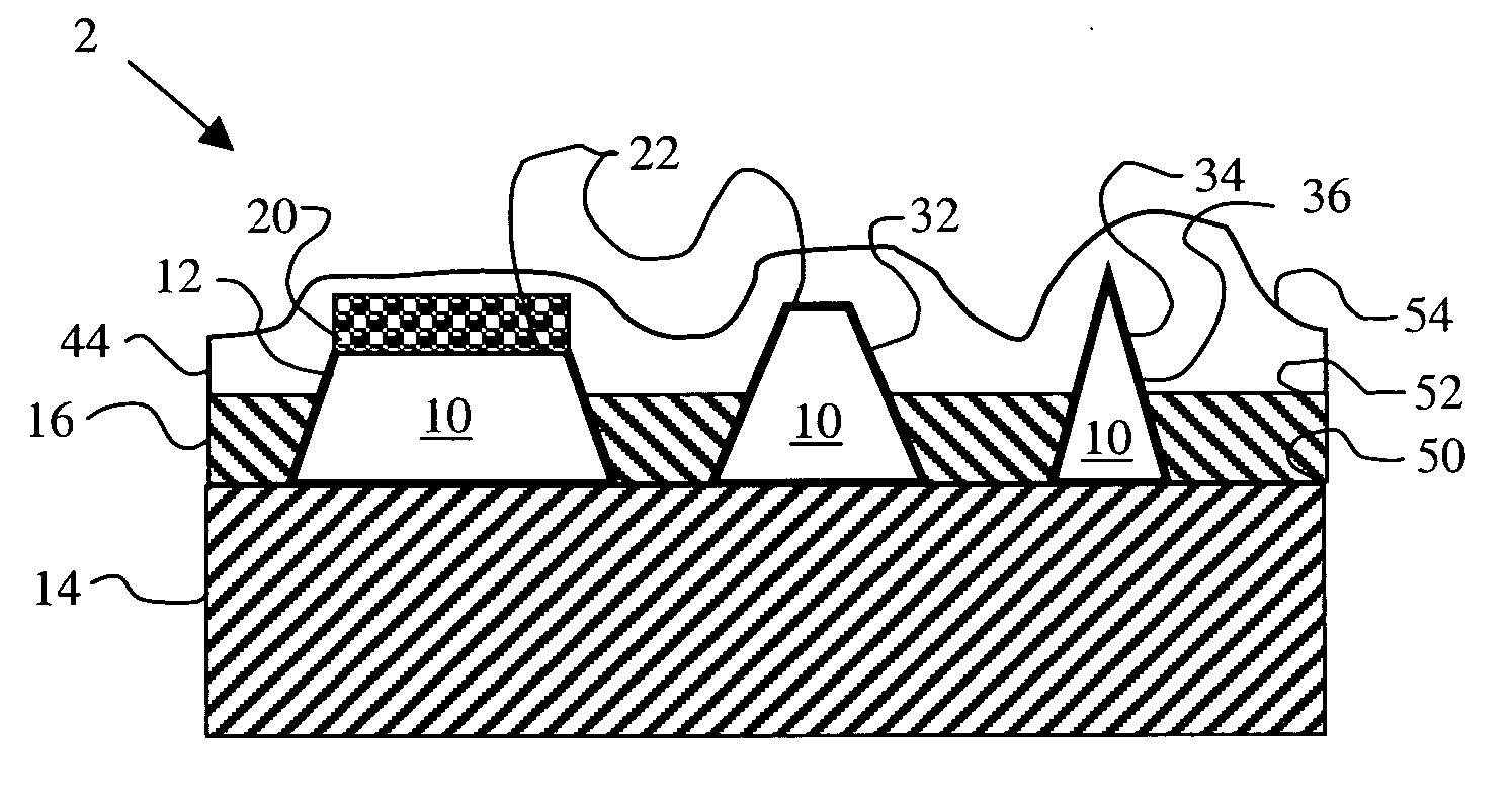
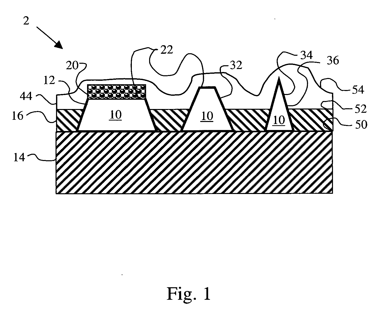
[0138] Four arrays of faceted structures (Samples 1, 2, 3 and 4) are prepared as in Example 1 except on a sapphire substrate having back metallization rather than an SEM anode. The faceted structures are arranged in an array that is two dimensional and planar (see FIG. 6). The exposed facet of the truncated faceted structures differs from one portion of the array to another portion of the array (X-Y direction) such that the ratio of polar surface area to non-polar surface area is based on the position of the faceted structure in the array. The exposed facets are polar c-plane naturally occurring planar faces.
[0139] Onto each of the exposed facets of sample 1 are disposed a sensor layer that includes a catalyst component. In this instance, the catalyst includes a metal, and particularly a catalyst component that interacts with ethanol. In the presence of ethanol, the sensor layer mass changes the strain and / or electrical properties of the surface of each faceted struct...
example 3
Exclusion Layers
[0150] Several arrays of faceted structures (samples 4-6) are prepared as in Example 2 Sample 1 with the exception that AlGaN is used rather than GaN. Over the sensor layer of each array an exclusion layer is deposited. For sample 4, a sol-gel process sets up a mesoporous frit having pores that are sized to be larger than ethanol but smaller than hexanol, in diameter and that are hydrophilic due to residual hydroxyls.
[0151] In sample 5, Lotus Effect layer is coated over the sensor layers. The Lotus Effect layer has both microscale structures, and nanoscale structures disposed on the microscale structures, that are hydrophobic and bound to the faceted structure array surface by a porous binder material. The structures are spaced from each other to provide the desired hydrophobic affect.
[0152] Surface hydrophilization using thermal oxidation in a dry atmosphere allows the deposition of highly mobile lipid membranes by vesicle fusion. In sample 6, a lipid bilayer is ...
PUM
 Abstract
Description
Claims
Application Information


