Porous chalcogenide thin film, method for preparing the same and electronic device using the same

a technology of porous chalcogenide and thin film, which is applied in the field of porous chalcogenide thin film, a method for preparing the thin film, and an electronic device, can solve the problems of low deposition speed, non-uniform morphology of the thin film, and applicability to processing, and achieve superior electrical properties to fabrication and crystallinity. high

Inactive Publication Date: 2007-04-26
SAMSUNG CORNING CO LTD
View PDF4 Cites 18 Cited by
  • Summary
  • Abstract
  • Description
  • Claims
  • Application Information

AI Technical Summary

Benefits of technology

[0018] In accordance with one aspect of the present invention, there is provided a porous chalcogenide thin film with a microporous structure that has greater crystallinity and can be applied as a s...

Problems solved by technology

However, this deposition method suffers from problems of low deposition speed and disadvantageous applicability to processing arising from the use of a chemical bath.
However, the ESAVD technique poses a problem in that the morphology of the thin films is non-uniform when compared with that of thin films prepared by spin coating.
Since the chalcogenide hydrazinium salt is chemically unstable it tends to deteriorate when stored over a period of time.
As a result, these methods are expensive and are not suitable for practical application...

Method used


Image

  • Porous chalcogenide thin film, method for preparing the same and electronic device using the same
  • Porous chalcogenide thin film, method for preparing the same and electronic device using the same
  • Porous chalcogenide thin film, method for preparing the same and electronic device using the same

Examples


example 1

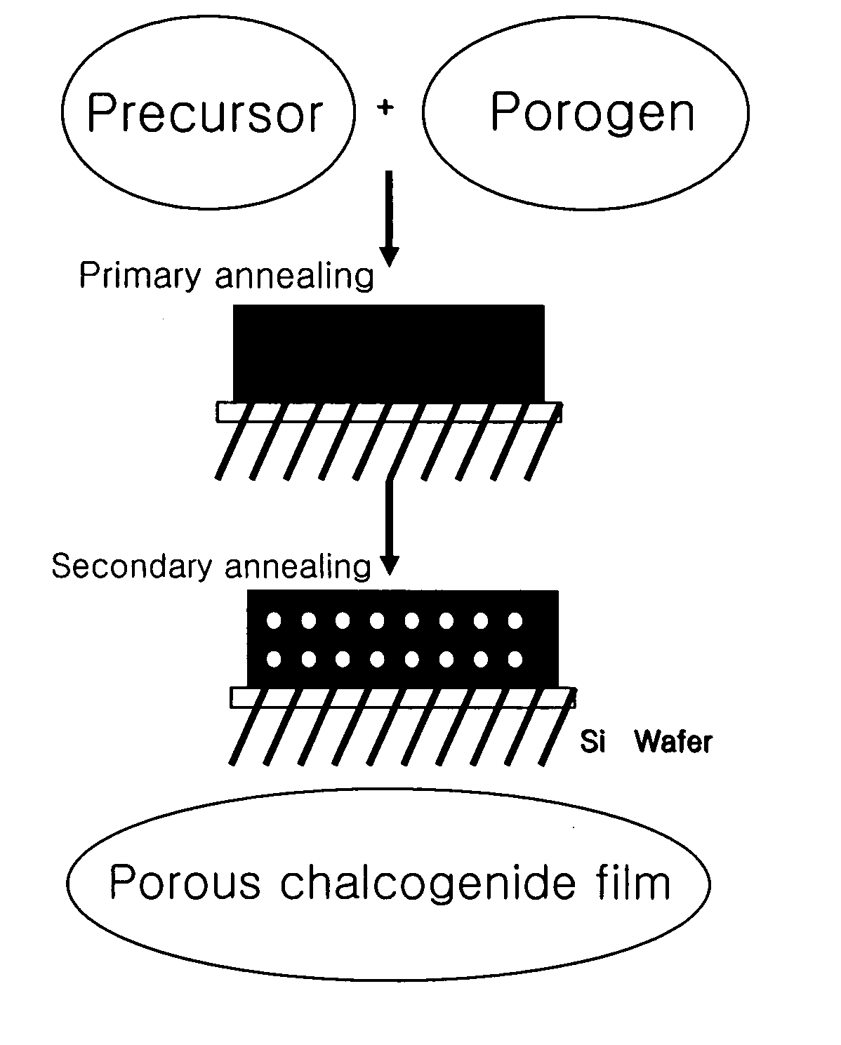
[0073] First, 0.2 g of the chalcogenide precursor compound prepared in Preparative Example 1 and 0.02 g of a-cyclodextrin were dissolved in 1.8 g of pyridine. The solution was stirred to prepare a precursor solution for the preparation of a porous chalcogenide thin film. The coating solution was spin-coated at 500 revolutions per minute (rpm) on a 4 inch silicon wafer for 20 seconds, baked on a hot plate in a nitrogen atmosphere at 100° C. for one minute, and dried to obtain a film. The dried film was annealed in a nitrogen atmosphere at 200° C. for 5 minutes, and further annealed under a vacuum at 400° C. for one hour to prepare a porous chalcogenide thin film.

examples 2-4

[0074] Porous chalcogenide thin films were prepared in the same manner as in Example 1, except that 0.04 g, 0.06 g and 0.08 g of a-cyclodextrin each was used to prepare four precursor solutions.


PUM


Abstract

A porous chalcogenide thin film having a microporous structure, a method for preparing the chalcogenide thin film and an electronic device employing the chalcogenide thin film, are provided. The porous chalcogenide thin film has superior crystallinity and can be applied as a semiconductor layer having superior electrical properties to the fabrication of devices by inserting functional metal or semiconductor nanoparticles into nanopores of the thin film.

Description

BACKGROUND OF THE INVENTION [0001] This non-provisional application claims priority under 35 U.S.C. §119(a) to Korean Patent Application No. 2005-100131 filed on Oct. 24, 2005, the entire contents of which are hereby incorporated by reference. [0002] 1. Field of the Invention [0003] The present invention relates to a porous chalcogenide thin film, a method for preparing the thin film, and an electronic device that employs the thin film. More specifically, the present invention relates to a microporous chalcogenide thin film containing pores between 1 and 50 nanometers (nm) in size, a method for preparing the porous chalcogenide thin film using a chalcogenide precursor compound and a porogen that is soluble in organic solvents by a solution coating process, e.g., spin coating or dip coating, and a composition for use in the preparation of the chalcogenide thin film. [0004] 2. Description of the Related Art [0005] Flat panel displays, such as liquid crystal displays and organic electr...

Claims


Application Information

Patent Timeline
IPC IPC(8): C01G11/02H01L29/08C07F3/00
CPCC07F3/003H01L21/32055H01L31/18H01L31/1828
Inventor JEONG, HYUN DAMSEON, JONG BAEKSHIN, HYEON JINHYUN, SANG HEON
Owner SAMSUNG CORNING CO LTD
Why Eureka
Try Eureka