

Silicon carbide semiconductor device and manufacturing method therefor
a technology of silicon carbide and semiconductors, applied in semiconductor devices, semiconductor/solid-state device details, electrical devices, etc., can solve the problems of device breaking, device dislocation, and large increase in power loss inside the device, so as to reduce the supersaturation on the growth surface, suppress the propagation of basal plane dislocation from the substrate to the epitaxial film, and prevent forward voltage deterioration
- Summary
- Abstract
- Description
- Claims
- Application Information
AI Technical Summary
Benefits of technology
Problems solved by technology
Method used
Image

Examples
first embodiment
[0101] (First Embodiment)
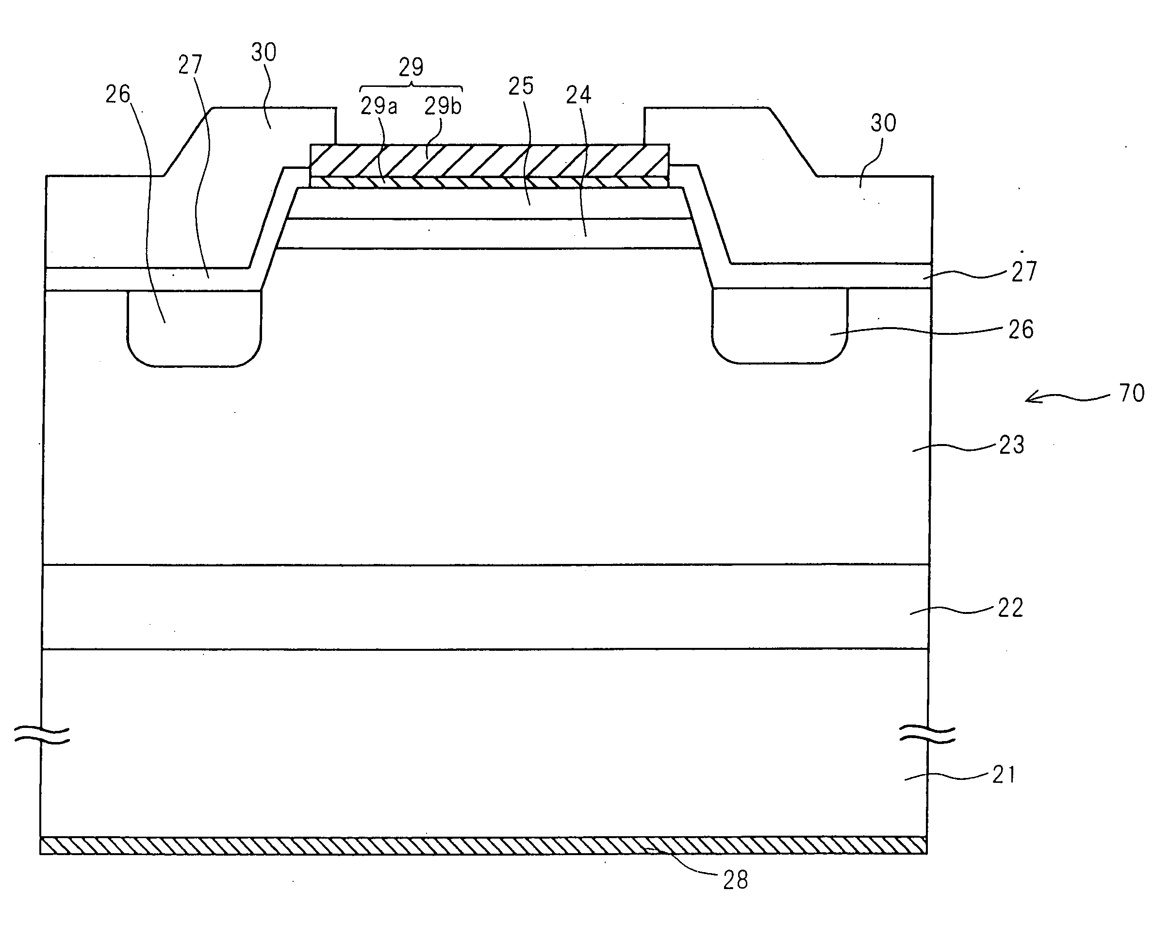
[0102]FIG. 1 is a sectional view of a pn (pin) junction diode which is a First Embodiment of a bipolar semiconductor device of the present invention. In this Embodiment, semiconductor layers to be described below are formed on an n-type (first conductive type) 4H SiC substrate 21 whose surface orientation has an off-angle of 8 degrees from the (000-1) carbon surface. In the term “4H,” the character “H” means hexagonal crystal and the numeral “4” means a crystal structure whose atomic lamination is four-layer cyclic. The C surface of the substrate 21 is a surface 2a having an off-angle θ of 8 degrees from the (000-1) carbon surface 2 of SiC crystal of FIG. 6. The film growth rate for each layer is 15 μm / h, where the increasing rate of film thickness per hour (h) is faster than in the conventional counterpart. Then, as described in detail below, n-type (first conductive type) 4H-SiC and p-type (second conductive type) 4H-SiC are epitaxially grown one by one, b...
third embodiment
[0150] (Third Embodiment) A Third Embodiment relates to an IGBT (Insulated Gate Bipolar Transistor) which is a bipolar semiconductor device of the -present invention. FIG. 5 is a sectional view of an IGBT 60 of this Embodiment. In this Embodiment, a substrate 61 (hereinafter, referred to as C surface substrate) using n-type 6H SiC whose surface orientation has an off-angle θ of 3.5 degrees from the (000-1) carbon surface 2 in FIG. 6 is prepared. On the substrate 61, three layers, i.e. a p-type 6H-SiC layer, an n-type 6H-SiC layer and a p-type 6H-SiC layer, are epitaxially grown in this order with a film-thickness increasing rate per hour (h) of 15 μm / h, by which an IGBT 60 is fabricated as is explained in detail below. The primary junction surface (a surface extending horizontally in the figure) of the p and n layers is the {0001} surface.
[0151] A comparative IGBT for comparison with the IGBT of this Embodiment is fabricated in the following way. A substrate (hereinafter, referred t...
PUM
| Property | Measurement | Unit |
|---|---|---|
| off-angle | aaaaa | aaaaa |
| angle | aaaaa | aaaaa |
| forward voltage | aaaaa | aaaaa |
Abstract
Description
Claims
Application Information