Reactor surface passivation through chemical deactivation

a passivation and reactor surface technology, applied in the direction of chemically reactive gases, crystal growth process, polycrystalline material growth, etc., can solve the problems of destroying the self-limiting nature of deposition, film buildup can delaminate from the reactor surface, contaminating the substrate surface,

Active Publication Date: 2007-05-03
ASM IP HLDG BV
View PDF21 Cites 54 Cited by
  • Summary
  • Abstract
  • Description
  • Claims
  • Application Information

AI Technical Summary

Problems solved by technology

A shorter duration purge step can increase the available time for adsorption and reaction of the reactants within the reactor, but the vapor phase reactants are not allowed to mix to avoid the risk of CVD reactions destroying the self-limiting nature of the deposition.
The film buildup can delaminate from the reactor surfaces and contaminate the substrate surface.
Hence, this can also increase the pulse and purge time required to saturate the wafer surface
On the other hand, cooler CVD reactant parts may be subject to reactant condensation or adsorption / desorption, as in ALD reactors, leading to contamination problems again.
Frequent cleaning of the reactor can limit the potential for contamination.
However, the reactor is out of service during these cleanings and thus reduces the efficiency of the ALD or CVD process.

Method used


Image

  • Reactor surface passivation through chemical deactivation
  • Reactor surface passivation through chemical deactivation
  • Reactor surface passivation through chemical deactivation

Examples


Embodiment Construction

,” one will understand how the features of this invention provide several advantages to vapor deposition methods and systems.

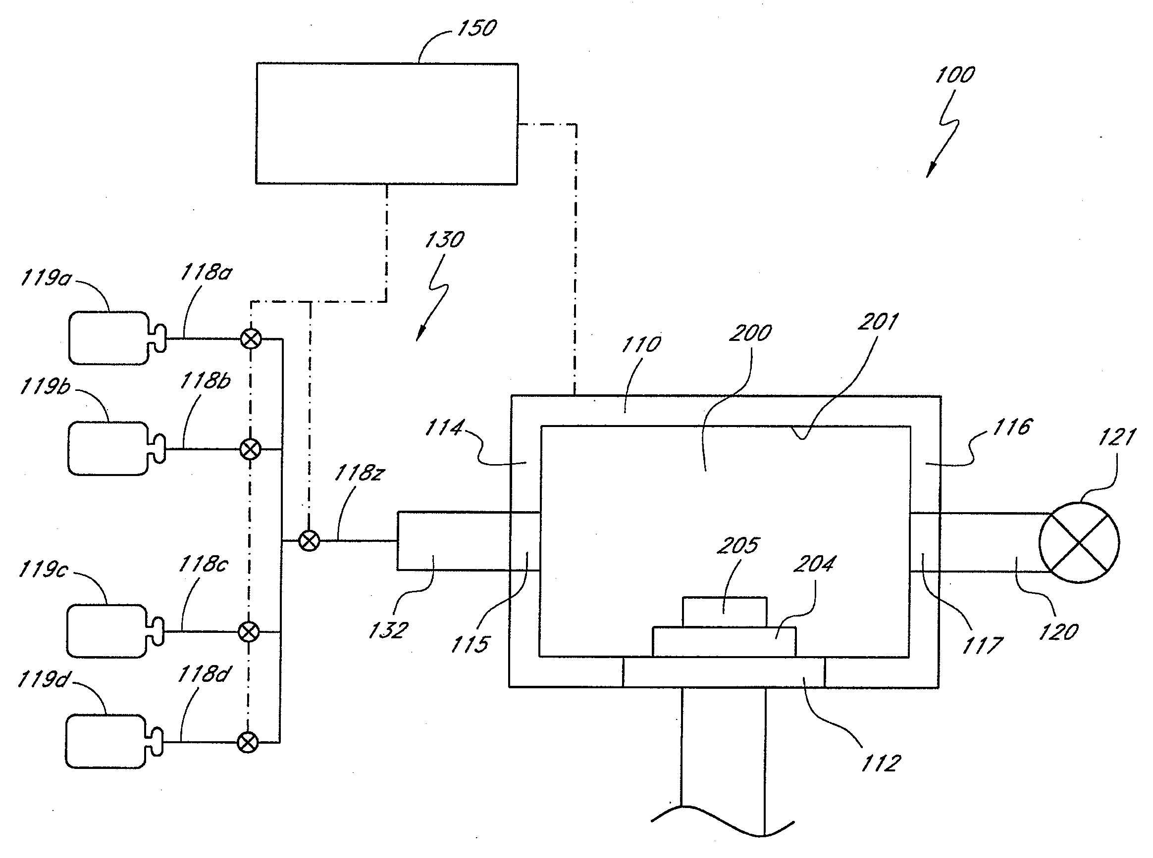
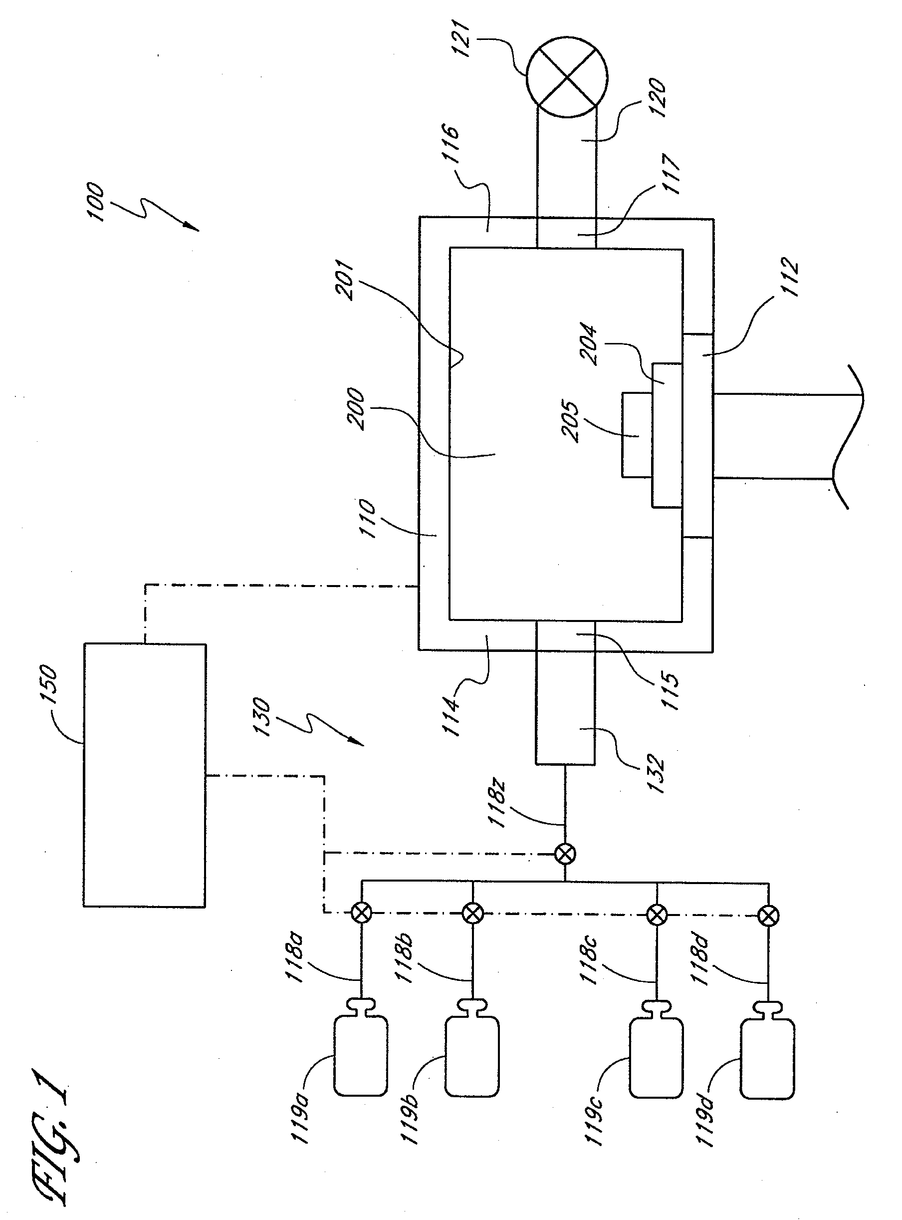
[0010] According to one aspect of the invention, a method is provided for deactivating surfaces of a vapor deposition reaction space. The surfaces are treated to render the vapor deposition process conducted therein selective to the substrate, rather than the treated surfaces. In one embodiment, treatment comprises an ex situ treatment prior to assembly of the parts defining the reaction space. In another embodiment, treatment and periodic re-treatment can be conducted in situ by flowing a treatment gas through the reaction space to deactivate reaction space surfaces.

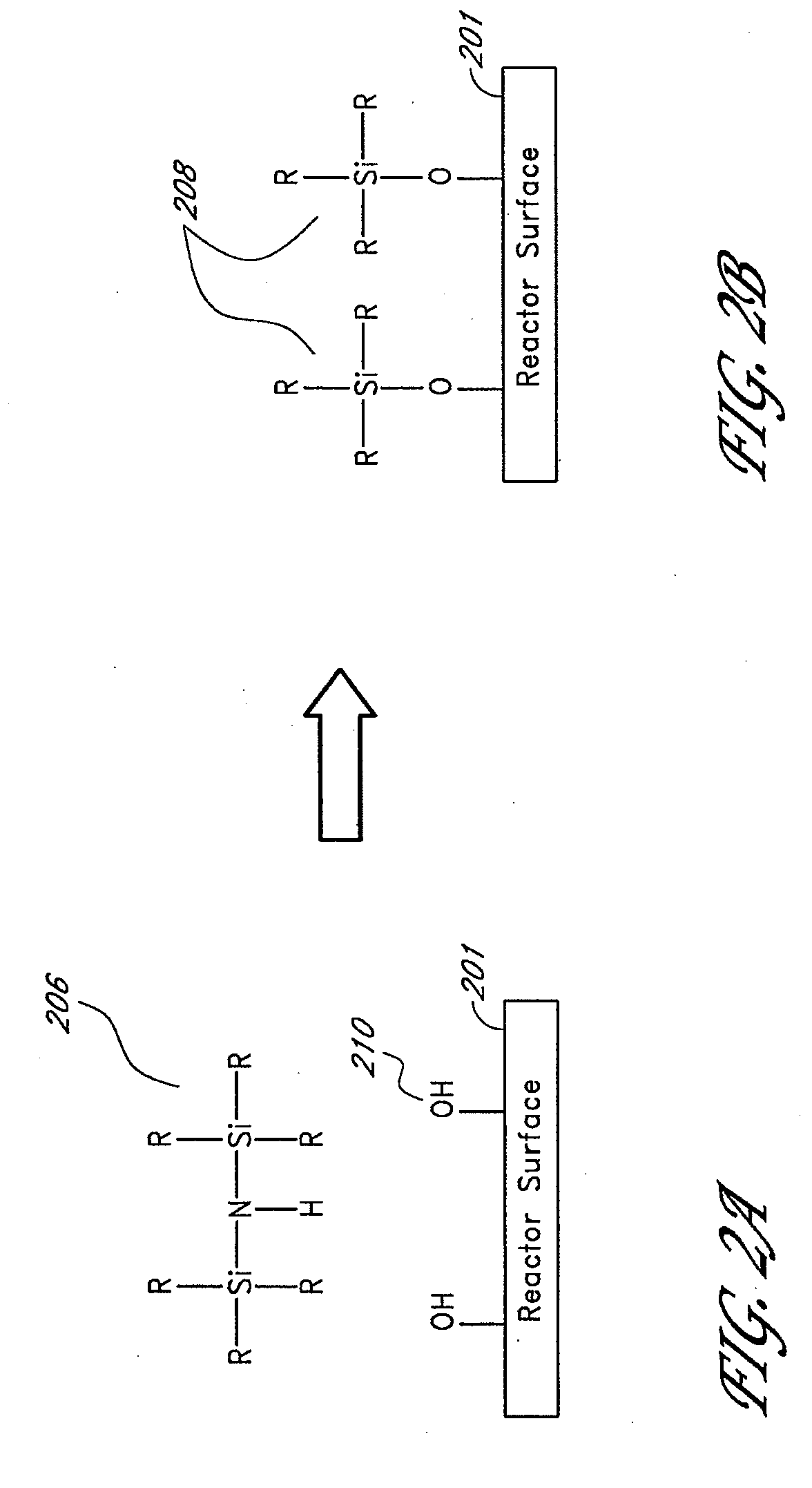
[0011] In accordance with another aspect of the invention, a vapor deposition reactor is provided with at least some of the surfaces that define a reaction space being deactivated by a monolayer that inhibits deposition reactions thereon. In the example of an atomic layer deposition (ALD) reactor...


PUM

PropertyMeasurementUnit
hydrophobicaaaaaaaaaa
thicknessaaaaaaaaaa
depositionaaaaaaaaaa

Abstract

Protective layers are formed on a surface of an atomic layer deposition (ALD) or chemical vapor deposition (CVD) reactor. Parts defining a reaction space for an ALD or CVD reactor can be treated, in situ or ex situ, with chemicals that deactivate reactive sites on the reaction space surface(s). A pre-treatment step can maximize the available reactive sites prior to the treatment step. With reactive sites deactivated by adsorbed treatment reactant, during subsequent processing the reactant gases have reduced reactivity or deposition upon these treated surfaces. Accordingly, purge steps can be greatly shortened and a greater number of runs can be conducted between cleaning steps to remove built-up deposition on the reactor walls.

Description

REFERENCE TO RELATED APPLICATION [0001] This application is continuation-in-part of U.S. patent application Ser. No. 11 / 539,312, filed Oct. 6, 2006, which is a divisional of U.S. patent application Ser. No. 10 / 841,585, filed May 7, 2004, which claims the priority benefit under 35 U.S.C. §119(e) to provisional patent application No. 60 / 469,181, filed May 9, 2003, the entire contents of these applications are hereby incorporated by reference herein.FIELD OF THE INVENTION [0002] The present invention generally relates to inhibiting deposition on reactor surfaces in chemical vapor deposition (CVD) and atomic layer deposition (ALD) reactors. More specifically, the present invention relates to de-activating a surface of the reactor to limit coating by subsequent gases flowing through the reactor. BACKGROUND OF THE INVENTION [0003] Atomic layer deposition (ALD) is a known process in the semiconductor industry for forming thin films of materials on substrates such as silicon wafers. ALD is ...

Claims


Application Information

Patent Timeline
Patent Type & Authority Applications(United States)
IPC IPC(8): C23C16/00
CPCB82Y30/00C23C16/4404C23C16/45525
Inventor VERGHESE, MOHITHSHERO, ERIC J.
Owner ASM IP HLDG BV
Why Eureka
Try Eureka