Field effect transistor and method of fabricating the same

a field effect transistor and field effect technology, applied in the field of thin film transistors, can solve the problems of large number of substrate materials that are otherwise useful that cannot be used, amlcd resin films that are useful to meet such demands or requests are difficult to use in fabrication process steps, and the organic semiconductor layer has further lowered the carrier mobility and hence cannot be used as a

Inactive Publication Date: 2007-05-17
PANASONIC CORP
View PDF3 Cites 42 Cited by
  • Summary
  • Abstract
  • Description
  • Claims
  • Application Information

AI Technical Summary

Benefits of technology

[0029] An active-matrix display according to the present invention comprises a plurality of field effect transistors as recited in any one of claims 1 to 15 which are disposed as switching devices for driving pixels.
[0030] A wireless ID tag according to the present invention comprises a field effect transistor as rec

Problems solved by technology

Because various materials and processing methods for forming an active-matrix liquid crystal display (AMLCD) based on an amorphous silicon (a-Si:H) or low-temperature formed polysilicon device require many fabrication process steps at high temperatures, a large number of substrate materials that are otherwise useful cannot be employed.
However, plastic sheets or resin films for AMLCDs which are useful to meet such demands or requests are difficult to use in fabrication process steps at temperatures of from 150° to 250° or higher.
If the organic semiconductor layer has increased grain boundary or lowered crystallinity, the organic semiconductor layer has further lowered carrier mobility and hence cannot be used as a TFT.
However, such a material is low in carrier mobility since the material is amorphous (see, for example, Takeo Kawase and two others, IDW '02, AMD2/EP1-1, pp.
A TFT having a semiconductor layer exhibiti

Method used


Image

  • Field effect transistor and method of fabricating the same
  • Field effect transistor and method of fabricating the same
  • Field effect transistor and method of fabricating the same

Examples


first embodiment

[0050] The first embodiment is directed to a TFT having a semiconductor layer formed from a composite material comprising an organic semiconductor material and nanotubes.

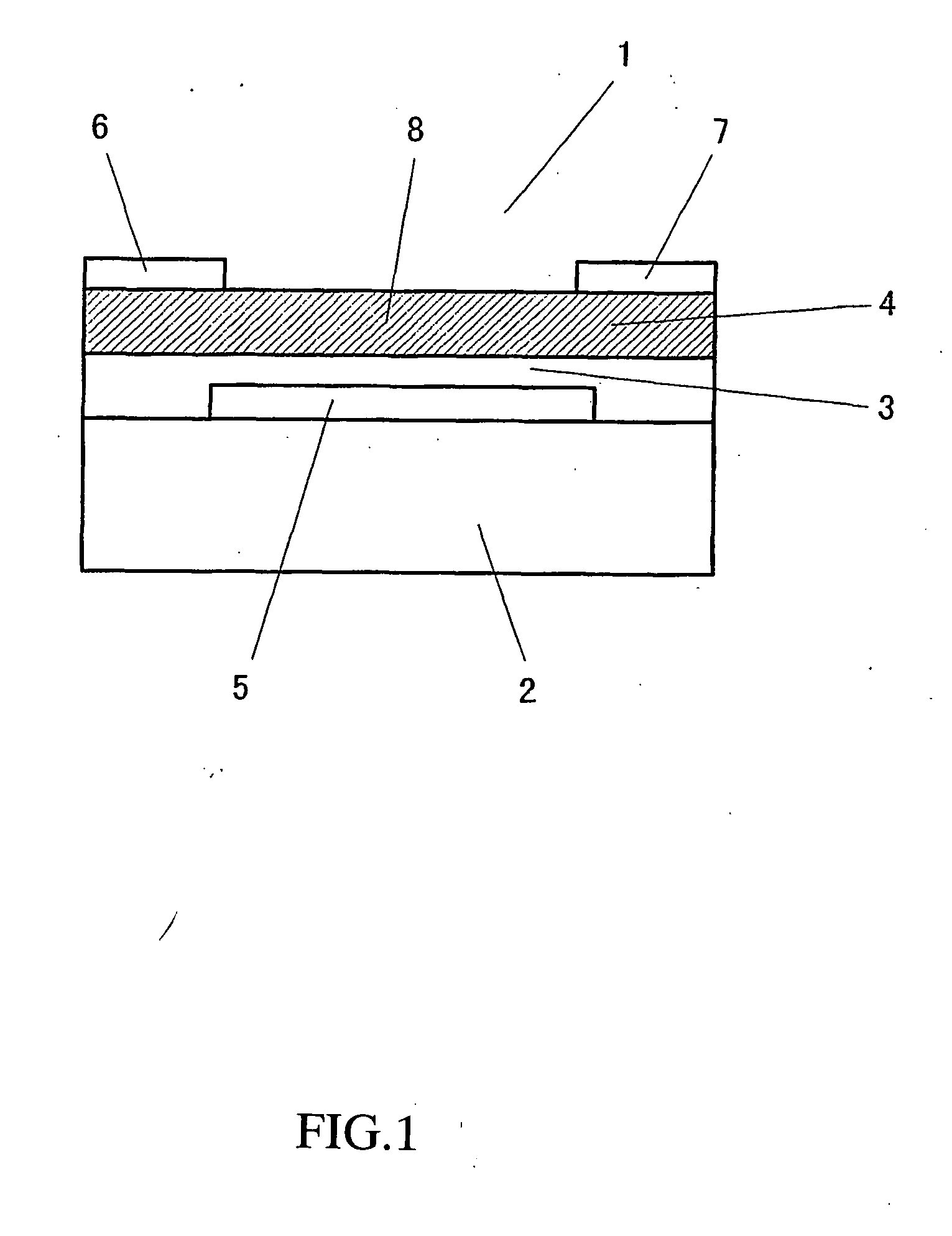
[0051]FIG. 1 is a sectional view schematically showing the construction of the TFT according to this embodiment. As shown in FIG. 1, the TFT 1 has, on a substrate 2, a gate electrode 5, a gate insulator 3, a semiconductor layer 4, a source electrode 6, and a drain electrode 7. Specifically, the gate electrode 5 is provided on a major surface of the substrate 2 and the gate insulator 3 is formed to cover the gate electrode 5. Further, the semiconductor layer 4 is provided on the gate insulator 3, while the source electrode 6 and the drain electrode 7 disposed separately from each other on the semiconductor layer 4. In a plan view, the gate electrode 5 is located intermediate the source electrode 6 and the drain electrode 7. With this construction, the gate electrode 5 is isolated from channel 8 to be electrically fo...

second embodiment

[0076] The second embodiment is directed to a TFT having a semiconductor layer formed from a composite material comprising an organic semiconductor material and nanotubes.

[0077]FIG. 4 is a sectional view schematically showing the construction of the TFT according to this embodiment. As shown in FIG. 4, the TFT 15 has, on a substrate 2, a gate electrode 5, a gate insulator 3, a source electrode 6, a drain electrode 7, and a semiconductor layer 16. Specifically, the gate electrode 5 is provided on a major surface of the substrate 2 and the gate insulator 3 formed to cover the gate electrode 5. The source electrode 6 and the drain electrode 7 are disposed separately from each other on the gate insulator 3, while the semiconductor layer 16 formed to cover the source electrode 6, drain electrode 7 and gate insulator 3. In a plan view, the gate electrode 5 is located intermediate the source electrode 6 and the drain electrode 7. With this construction, the gate electrode 5 is isolated fr...

third embodiment

[0087] The third embodiment is directed to a TFT having a semiconductor layer formed from a composite material comprising an organic semiconductor material and nanotubes.

[0088]FIG. 6 is a sectional view schematically showing the construction of the TFT according to this embodiment. As shown in FIG. 6, the TFT 20 is a top-gated TFT having, on a substrate 2, a source electrode 6, a drain electrode 7, a semiconductor layer 13, a gate insulator 3, and a gate electrode 5. Specifically, the source electrode 6 and the drain electrode 7 are disposed separately from each other on a major surface of the substrate 2, while the semiconductor layer 13 formed to cover the source electrode 6, drain electrode 7 and substrate 2. The gate insulator 3 is provided over the semiconductor layer 13, while the gate electrode 5 provided on the gate insulator 3. In a plan view, the gate electrode 5 is located intermediate the source electrode 6 and the drain electrode 7. With this construction, the gate ele...


PUM


Abstract

A field effect transistor according to the present invention has a semiconductor layer through which carriers injected from a source region travel toward a drain region, the semiconductor layer being formed from a composite material including an organic semiconductor material and nanotubes. The nanotubes may be nanotubes including plural ones joined with each other.

Description

TECHNICAL FIELD [0001] The present invention relates to a field effect transistor and a method of fabricating the same and, more particularly, to a thin film transistor and a method of fabricating the same. BACKGROUND ART [0002] Presently, field effect thin film transistors (hereinafter will be referred to as TFTs as the case may be) are being suitably used as driving devices for use in flat panel displays and the like. Though various TFT configurations have been proposed, TFTs generally have a basic configuration wherein current passing between source and drain electrodes in contact with a semiconductor layer is controlled by means of voltage applied to a gate electrode formed on the semiconductor layer via an insulating layer (that is, by means of an electric field generated by the applied voltage). Usually, such a TFT is fabricated using a thin film control process by which layers on a substrate are processed and formed under precise control. Such TFTs call for excellent electric...

Claims


Application Information

Patent Timeline
IPC IPC(8): H01L29/76H01L27/32H01L51/00H01L51/30
CPCB82Y10/00H01L27/3244H01L51/0048H01L51/0545H01L51/0595H10K59/12H10K85/221H10K10/466H10K10/701
Inventor NANAI, NORISHIGEWAKITA, NAOHIDETAKEUCHI, TAKAYUKI
Owner PANASONIC CORP
Why Eureka
Try Eureka