System and method for positioning and synthesizing of nanostructures

a nanostructure and positioning technology, applied in the field of nanostructure formation methods, can solve the problems of many of these advantages only being possible, progress only being truly achieved, and techniques not practical

Inactive Publication Date: 2007-05-17
PENN STATE RES FOUND
View PDF8 Cites 16 Cited by
  • Summary
  • Abstract
  • Description
  • Claims
  • Application Information

AI Technical Summary

Problems solved by technology

However, many of these advantages are only possible if the position of the nano-structure is precisely controlled.
However, progress is only truly achieved when these building blocks are assembled into useful systems.
However, such techniques are not practical and usually time consuming.
In addition, the techniques are not environmentally safe since only few out of a large number of grown nanostructures are used for the assembly and the unused nanostructures are discarded.
Most of these techniques are also not practical or not controllable, or both.
However, this method does not provide a high density of assembled nanocolloids because of the repulsive force caused by electrical charges.
This approach only works for a layer and does not provide any controllable nanostructure positioning at a selected location.
However, their method is not practical since it requires repeated use of e-beam lithography and the nano-structure positioning process is slow.
In this approach, the direction of the nano-structure positioning is random and the positioned structure has a significant, unwanted branching structure.

Method used


Image

  • System and method for positioning and synthesizing of nanostructures
  • System and method for positioning and synthesizing of nanostructures
  • System and method for positioning and synthesizing of nanostructures

Examples


example 1

Formation of a Nanoparticle Ensemble Using a Reusable Template Structure

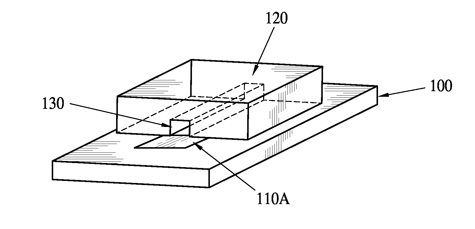
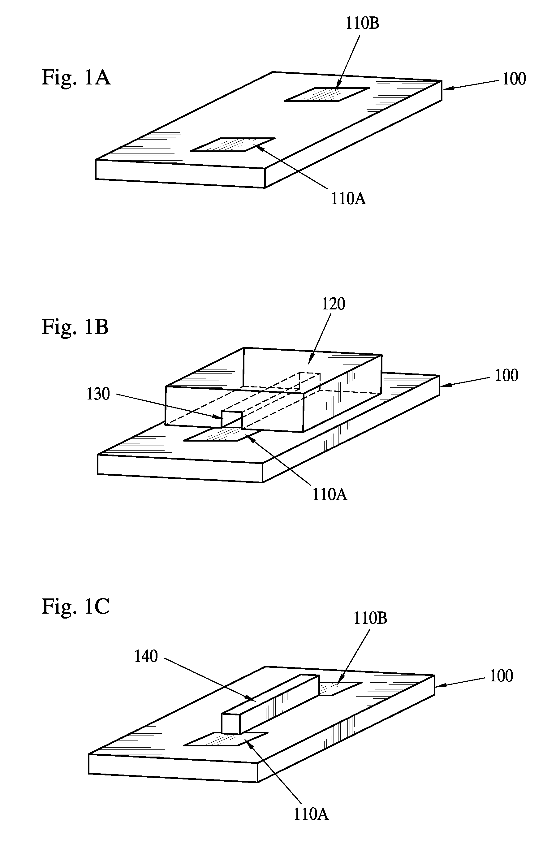
[0047] As a demonstration of the temporary-template approach to positioning nano-structures, a single-layered polydimethylsiloxane (PDMS) reusable template structure without an electrode structure was prepared. Even though it is desirable to use the double PDMS layers, a single PDMS layer was used for the specific example since the single layer worked fine in the scale of larger than 10 um. A pattern of the template structure was defined on a gold film coated silicon wafer (the master) using standard lithography to create a mold to make a PDMS reusable template structure which had no template floor for the channels. The reusable template structure features found on the master were produced using etching. The feature dimensions were 25 μm in width, 20 μm in height, and 2 cm in length. A PDMS solution was used for casting the reusable template structure.

[0048] When PDMS is used, the reusable template structure m...

example 2

Formation of a Nano-Structure Through Electropolymerization

[0050] Polyaniline wires were grown on a silicon nitride coated silicon wafer using a steppable PDMS template and electropolymerization. The PDMS template plate, having three different channel widths (5 μm, 1 μm, and 0.5 μm), initially was positioned between two electrodes (anode and cathode) that were already formed on the substrate using dry etching, metal evaporation and lift-off. Three different widths (5 μm, 1 μm, and 0.5 μm) of nanowires were grown. These “step-and-grow” polyaniline nanowires showed conductivities of ˜10 S / cm.

[0051] In the growth step, an aniline monomer dissolved in HCl solution, preferably about 0.3 M aniline in about 0.75 M HCl, was applied to the ends of the channels in the template. The monomer was introduced via capillary action into the channel structures formed by the template and the substrate top surface. Electropolymerization was then performed using the electrodes by applying about 1V of ...

example 3

Growth of Nanowires Using an External Electrode Structure

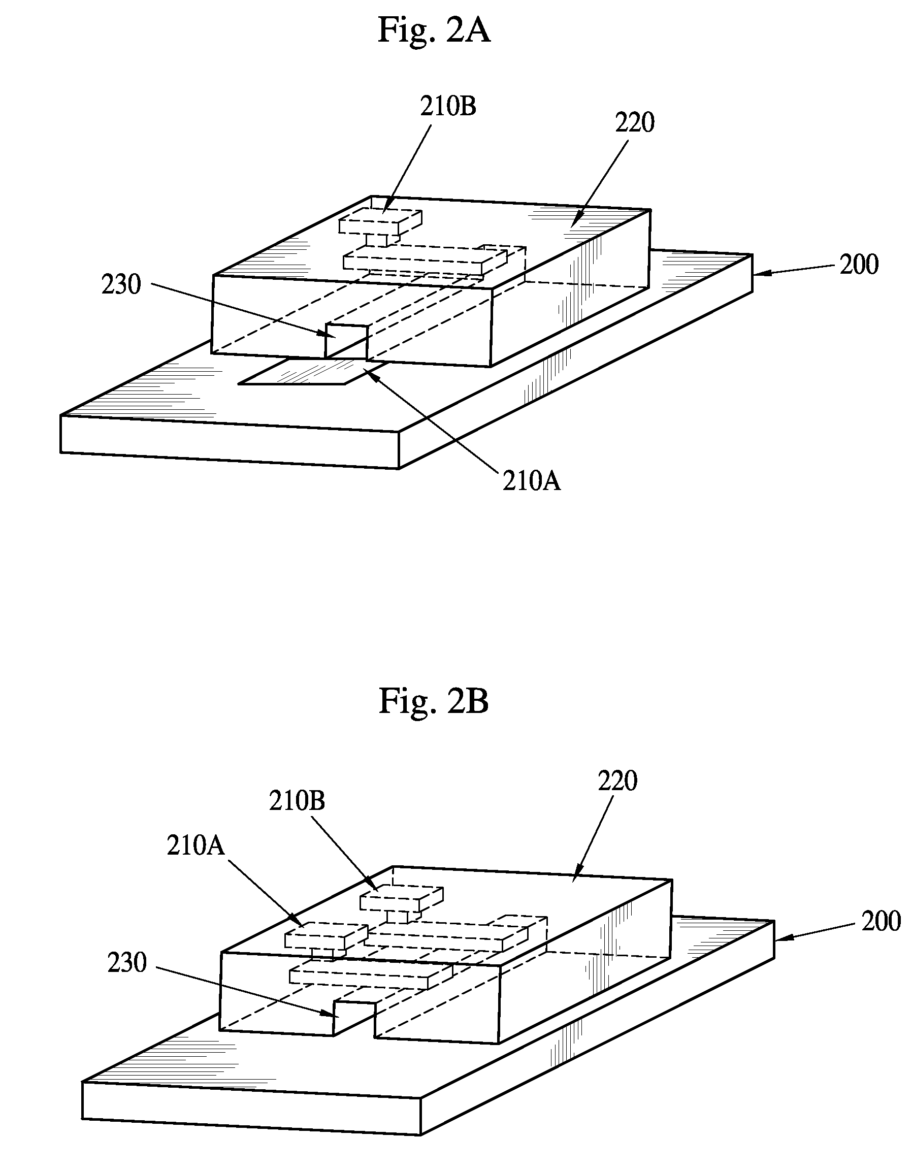
[0052] The configuration illustrated in FIG. 3A was used to grow tin nanowires. In particular, the reusable template structure was positioned on a substrate that had four electrode structures predisposed thereon. About 5 ul of commercially available Sn plating solution (purchased from Trensene, Inc.) was applied to the side of the reusable template structure. The electrode structure positioned on the substrate (i.e. electrode structure 310A) and the external electrode (i.e. electrode structure 310B) were connected to an HP4145 using two manipulator probes in an I-V station. In this exemplary demonstration, the external electrode was consumable (i.e., it was tin). A voltage of −0.075V was applied to the electrode structure positioned within the substrate, and a nanowire was grown for approximately 5 minutes. After the growing was complete, the electrical connections were disconnected and the reusable template structure was sep...


PUM

PropertyMeasurementUnit
diameteraaaaaaaaaa
heightaaaaaaaaaa
widthaaaaaaaaaa

Abstract

The invention relates to a method of forming at least one nano-structure with a reusable template structure having a channel. The method includes introducing at least one reagent into the channel, and reacting the at least one reagent to form a nano-structure within the channel. The nano-structure forming channel may be positioned in alignment with one or more electrode structures, which may be positioned within or upon the substrate, may be embedded in the reusable template structure, and / or may be external electrode structures positioned outside of the reusable template structure and independent of the substrate. In addition, the electrode structures may be a source material for the formation of the nano-structure in the channel.

Description

RELATED APPLICATION DATA [0001] This application claims priority to U.S. Provisional Patent Application 60 / 726,224, filed Oct. 14, 2005, which is hereby incorporated by reference in its entirety.FIELD OF THE INVENTION [0002] This invention relates to methods for forming nano-structures using reusable template structures. In addition, this invention relates to methods of positioning and forming nano-structures through the use of electrodes, including consumable electrodes. BACKGROUND OF THE INVENTION [0003] Nano-structures or nanoelements such as nanowires, nanoribbons, nanotubes, nanocolloids, nanotetrapods, nanodiscs, nanorods, nanobeads, and the like, attract a great deal of attention because of their huge potential in a wide range of applications from chemical / biological sensors to quantum electronic devices. The small size of these structures provides advantages ranging from enhanced integration in device fabrication to high detection sensitivity in sensor applications. However,...

Claims


Application Information

Patent Timeline
Patent Type & Authority Applications(United States)
IPC IPC(8): B01J19/00
CPCB01J31/124B01J35/0013B81B2207/07B81C1/00492B81C3/002C25D1/006B82Y10/00B82Y30/00B82Y40/00G03F7/0002C25D1/04B81C2201/0183
Inventor JOSHI, SANJAYFONASH, STEPHEN J.NAM, WOOK JUNGARG, PRANAV
Owner PENN STATE RES FOUND
Why Eureka
Try Eureka