Ultra broadband mirror using subwavelength grating

a subwavelength grating and ultra-broadband technology, applied in the field of wide-band mirrors, can solve the problems of difficult fabrication and limited tuning range of existing filters, and achieve the effects of high reflectivity, wide reflection spectrum, and scalable for different wavelengths

Active Publication Date: 2007-05-24
RGT UNIV OF CALIFORNIA
View PDF8 Cites 73 Cited by
  • Summary
  • Abstract
  • Description
  • Claims
  • Application Information

AI Technical Summary

Benefits of technology

[0015] The present invention generally comprises a sub-wavelength grating that has a very broad reflection spectrum and very high reflectivity. The design is scalable for different wavelengths, and facilitates monolithic integration of optoelectronic devices at a wide range of wavelengths from visible to far infrared.
[0018] Micro-electro-mechanical systems (MEMS) provide a simple wavelength tuning mechanism for many optoelectronic devices. The major advantages of MEMS-based tunable filters include a large tuning range, continuous tuning with high precision, a narrow passband and a fast response time (1-10 microseconds). The basic concept is based on scanning Fabry-Perot (FP) etalon with an integrated MEMS drive to provide precise physical change of the cavity length. A conventional etalon comprises two mirrors separated by a cavity gap. The filter can be tuned by moving one of the mirrors relative to the other changing the dimensions of the air gap. Thus, conventional MEMS-based tunable filters have the advantage of continuous tuning in that variation of the etalon gap size results in the variation in the transmission wavelength. However, existing filters have a limited tuning range (Δλ / λ˜7%) and have mechanical structures that have a small optical fill factor and are difficult to fabricate. The present invention provides a tunable filter using sub-wavelength grating structures as the reflectors that provides a much larger tuning range (Δλ / λ>30%) in the far-infrared wavelength (FIR) regime. It will be seen that the MEMS-based optical filter design is flexible and can be scaled to a wide range of wavelengths by simply changing the dimensions of the reflectors. The design also provides a large optical fill factor over existing designs that will permit the fabrication of two-dimensional arrays that require reasonably low driving voltages.

Problems solved by technology

However, existing filters have a limited tuning range (Δλ / λ˜7%) and have mechanical structures that have a small optical fill factor and are difficult to fabricate.

Method used


Image

  • Ultra broadband mirror using subwavelength grating
  • Ultra broadband mirror using subwavelength grating
  • Ultra broadband mirror using subwavelength grating

Examples


example 1

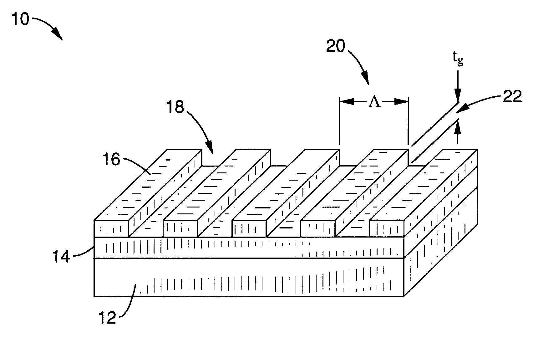
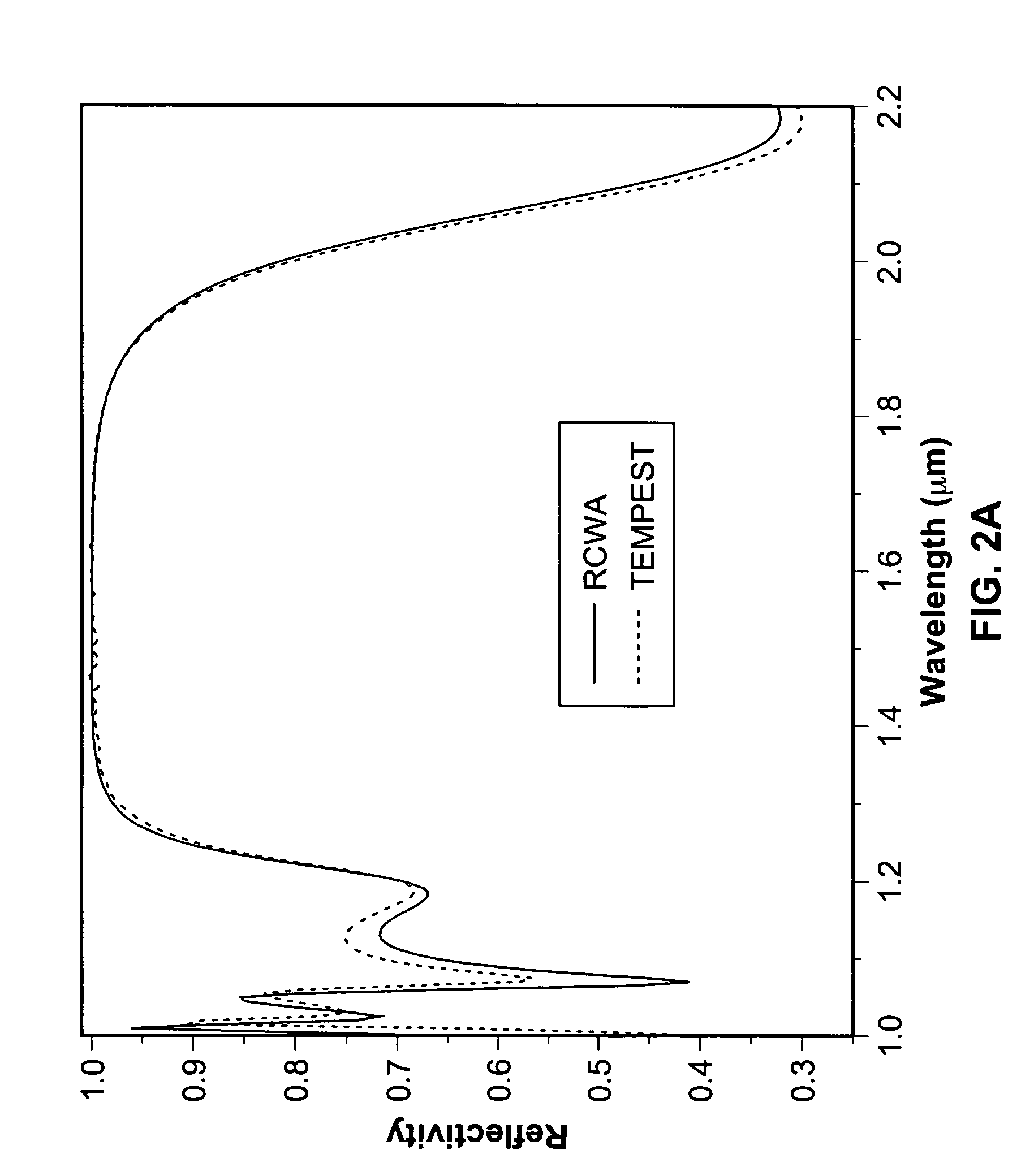
[0046] Turning now to FIG. 2A through 2D, the function of a sub-wavelength grating structure shown in FIG. 1 was simulated and evaluated. A very broadband mirror Δλ / λ>30%, with R>0.99, was obtained for wavelengths centered around 1.55 μm, over the range 1.33 μm to 1.80 μm, as depicted by FIG. 2(a). The reflection bandwidth of the mirror is also very broad for a higher reflectivity R>0.999 (1.40 μm to 1.67 μm or Δλ / λ>17%). The parameters used in the simulation were: Si substrate (n=3.48), grating period Λ=0.7 μm, high index material nn=3.48 (Poly-Si), low index material in and above the grating=1 (air), low index material under the grating nL=1.47 (SiO2), grating thickness tg=0.46 μm and grating duty cycle=0.75. The index of refraction was considered constant along the covered range, which is a very good approximation since most semiconductor materials such as Si, GaAs and ZnSe have index of refraction practically independent of wavelength in the considered ranges.

[0047]FIG. 2 illus...

example 2

[0058] In order to demonstrate the functionality of the design, several single wavelength grating structures according to FIG. 1 were fabricated. The 1D grating structures were formed with stripes of high index material disposed on two low index layers. The high index material was poly-Si (nh)=3.48, and the low index material within the grating was air (n=1). The low index material under the grating was SiO2 with (nL)=1.47 and a thickness (tL)=0.58 μm and (tg)=0.4 μm. The grating period was varied from 0.7 μm to 0.9 μm and the grating duty cycle was varied 40-80%. The duty cycle is defined as the ratio of the width of the high index material to the total period length. Fabrication was conducted on a silicon wafer and e-beam lithography on PMMA was used for lift off of metal as to mask the top oxide layer, which was etched by RIE. The grating is polarization sensitive and light polarized along the grating lines will not see the band gap. However, if the grating has a 2D symmetry it w...

example 3

[0063] A simple 1D grating was simulated to illustrate the scalability of the single wavelength grating structures and the dependence of reflectivity spectrum on various parameters. A very broadband mirror with reflectivity larger than 99% is obtained over the range of 1.4 μm to 1.7 μm (Δλ / λ>19%). The simulation calculations were performed based on Rigorous Coupled Wave Analysis (RCWA) and confirmed by time-domain electromagnetic propagation using TEMPEST®. The high index material was poly-Si (nh)=3.48, and the low index material within the grating was air (n=1). The low index material under the grating was SiO2 with (nL)=1.47 and a thickness (tL)=0.5 μm and (tg)=0.46 μm. The fill factor was 0.75. The grating period was 0.7 μm. The index of refraction was considered constant along the coverage range.

[0064] It can be seen that the period of the grating is sub-wavelength (but not half wavelength) and a scalable constant. Accordingly, the structure is scalable by multiplying the perio...


PUM


Abstract

A sub-wavelength grating structure that has a very broad reflection spectrum and very high reflectivity comprising segments made of high refractive index material disposed on a layer of low refractive index material and a low refractive index material disposed above and between the segments. The index differential between the high and low index materials determines the bandwidth and modulation depth. The larger difference in refractive indices gives rise to wider reflection bands. The reflection is sensitive to parameters such as the grating period, the grating thickness, the duty cycle of the grating, the refractive index and the thickness of the low index layer underneath the grating. The design is scalable for different wavelengths, and facilitates monolithic integration of optoelectronic devices at a wide range of wavelengths from visible to far infrared. The sub-wavelength grating reflectors may be used in a variety of settings such as tunable etalon filters and as a replacement for conventional distributed Bragg reflectors.

Description

CROSS-REFERENCE TO RELATED APPLICATIONS [0001] This application claims priority from, and is a 35 U.S.C. § 111(a) continuation of, co-pending PCT international application serial number PCT / US2005 / 001416, filed on Jan. 14, 2005, incorporated herein by reference in its entirety, which designates the U.S., which claims priority from U.S. provisional application Ser. No. 60 / 536,570, filed on Jan. 14, 2004, incorporated herein by reference in its entirety. [0002] This application is also related to PCT International Publication No. WO 2005 / 089098 A2 and WO 2005 / 089098 A3, each of which is incorporated herein by reference in its entirety.STATEMENT REGARDING FEDERALLY SPONSORED RESEARCH OR DEVELOPMENT [0003] This invention was made with Government support under a grant from DARPA (Center for Bio-Optelectronic Sensor Systems [BOSS]), Contract No. MDA9720010020. The Government has certain rights in this invention.INCORPORATION-BY-REFERENCE OF MATERIAL SUBMITTED ON A COMPACT DISC [0004] Not ...

Claims


Application Information

Patent Timeline
Patent Type & Authority Applications(United States)
IPC IPC(8): G02B5/18G02B27/42H01S5/14H01S5/183
CPCG02B5/0816G02B5/1809G02B5/1861G02B26/001G02B26/0808G02B26/0833G02B27/42G02B27/4255G02B27/4261H01S5/0655H01S5/18319H01S5/1835H01S5/18355H01S5/18366H01S5/187
Inventor CHANG-HASNAIN, CONNIE J.RONDINA MATEUS, CARLOS FERNANDOHUANG, MICHAEL CHUNG-YI
Owner RGT UNIV OF CALIFORNIA
Why Eureka
Try Eureka