Long-wavelength vertical cavity surface emitting lasers having oxide aperture and method for manufacturing the same

a laser and vertical cavity technology, applied in semiconductor lasers, laser details, electrical devices, etc., can solve the problems of low thermal conductivity of about 1/10, difficult use of gaas/algaas, and thick mirror layer growth, etc., to achieve easy manufacturing, low cost, and low cost

Inactive Publication Date: 2007-06-07
RAYCAN
View PDF3 Cites 7 Cited by
  • Summary
  • Abstract
  • Description
  • Claims
  • Application Information

AI Technical Summary

Benefits of technology

[0010] In the vertical cavity surface emitting laser device of the invention, lattice defects can be minimized by growing a layer containing a sufficient content of material, for example, Al, based on stable homogeneous-materials and sensitive to wet oxidation, adjustment of the thickness of an electric current shielding layer can be easily obtained via low temperature re-growth and epitaxy growth, and the process can be performed at a low temperature of about 400° C. for a short period of time of several minutes by means of the step of oxidizing an AlGaAs layer. In particular, the vertical cavity surface emitting laser device of the invention comprises the AlGaAs oxide layer, so that it can be very easily manufactured with high reliability and stability.

Problems solved by technology

However, for applications of wavelengths of 1.3 μm and 1.5 μm, which are mainly used for communication, it is difficult to use GaAs / AlGaAs, and thus, the vertical cavity surface emitting laser device is generally formed using InGaAsP or InAlGaAs on an InP substrate.
In addition, quaternary materials such as InGaAsP or InAlGaAs results in a low thermal conductivity of about 1 / 10 that of binary materials such as GaAs, and have many problems caused by difficulty in provision of the effective current confinement structure.
However, the monolithic method has disadvantages in that it is difficult to grow a thick mirror layer, and that quaternary materials are used, and therefore deteriorate the thermal properties.
However, after the activation layer and the mirror layer are separately grown by the epitaxy growth, a complicated process (for example, a wafer bonding process) is used to combine these components into the structure for the vertical cavity surface emitting laser device, causing bonding defects.
As a result, the hybrid method has problems of decreases in reliability and productivity along with an increase of manufacturing costs.
However, when manufacturing the long-wavelength vertical cavity surface emitting laser device, the ion-implantation process, the process for forming the electric current confining structure in the air gap, the process for forming the buried tunnel junction structure, the wafer bonding process, the process for forming an oxidation layer using an InAlAs layer and the like have problems in that a complicated process is required to form the electric current confining structure, and it is difficult to adjust the thickness of the electric current confining layer.

Method used


Image

  • Long-wavelength vertical cavity surface emitting lasers having oxide aperture and method for manufacturing the same
  • Long-wavelength vertical cavity surface emitting lasers having oxide aperture and method for manufacturing the same
  • Long-wavelength vertical cavity surface emitting lasers having oxide aperture and method for manufacturing the same

Examples


Embodiment Construction

[0023] Preferred embodiments of the present invention will be described in detail with reference to the accompanying drawings.

[0024] A method for manufacturing a long-wavelength vertical cavity surface emitting laser device in accordance with one embodiment of the present invention will be described as follows.

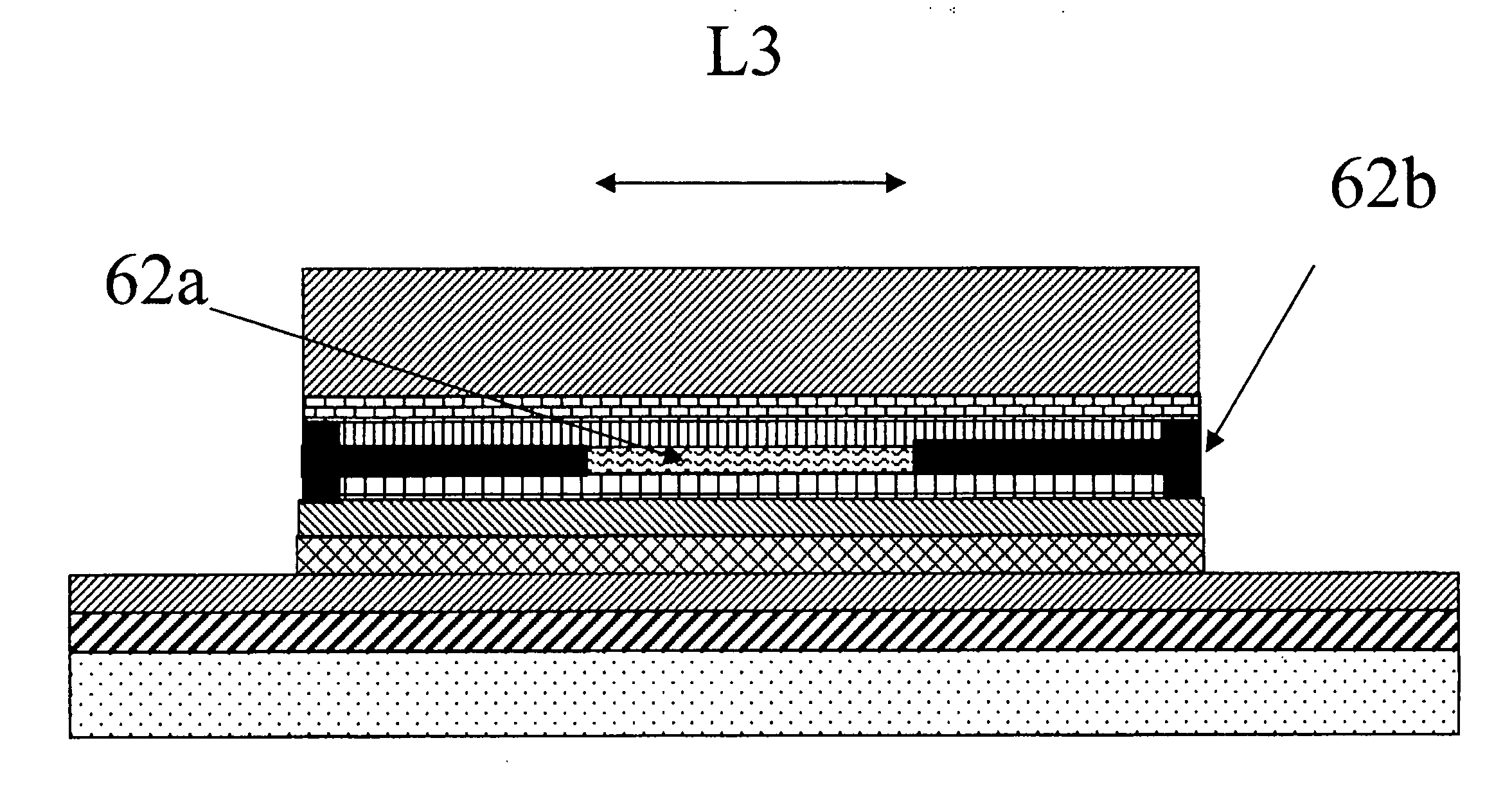
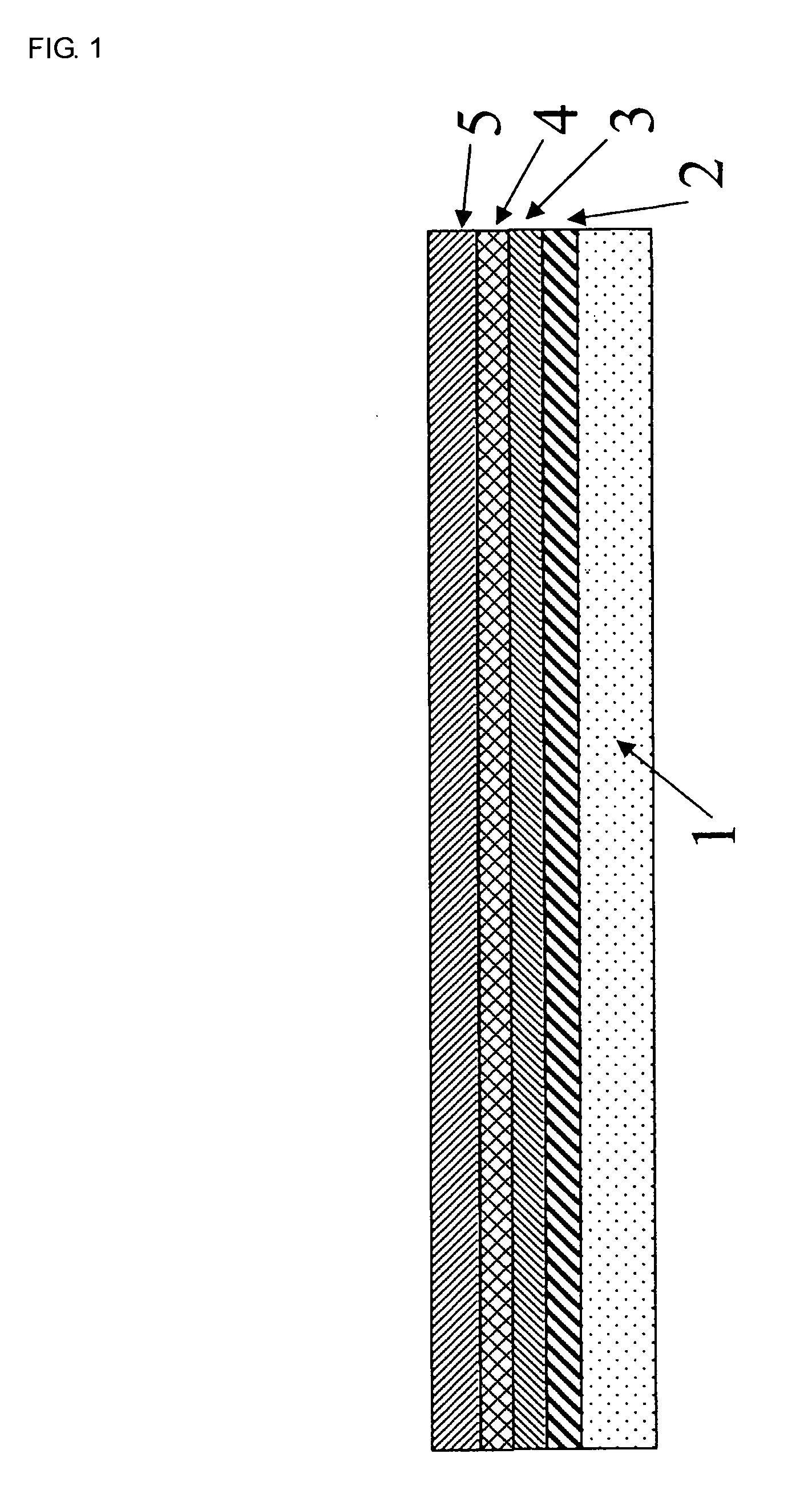
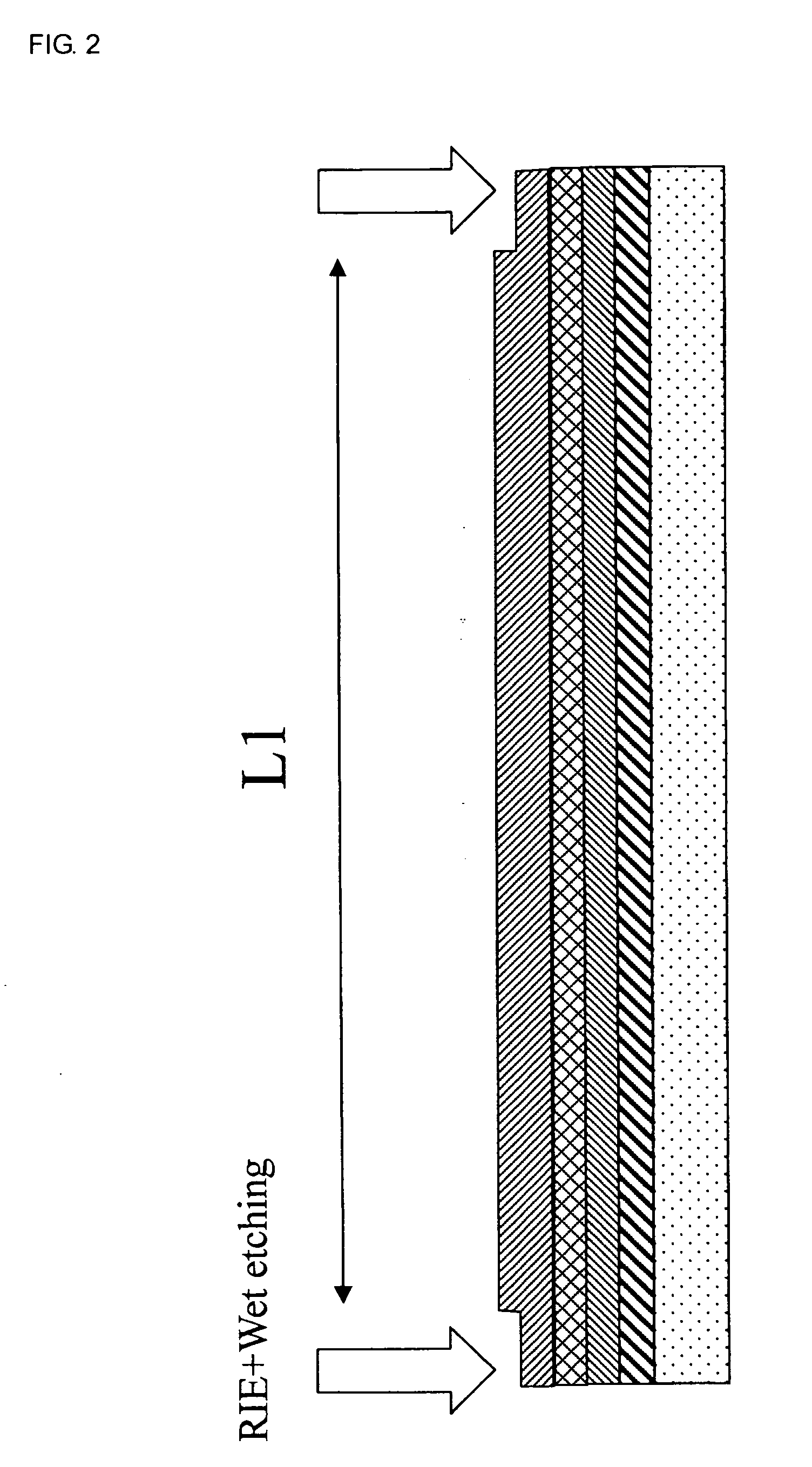
[0025] First, as shown in FIG. 1, in order to manufacture the long-wavelength vertical cavity surface emitting laser device of the invention, a semiconductor lower mirror layer 2 is grown on an InP substrate 1 by a compound-semiconductor epitaxy growth method, in which the semiconductor lower mirror layer 2 comprises InAlGaAs / InAlAs or InAlGaAs / InP. Then, a first semiconductor electrode layer 3 comprising n-InP, an optical gain-activation layer 4 constituted by an InAlGaAs multiple quantum-well layer, and a semiconductor anode layer 5 comprising p-InP are sequentially grown on the semiconductor lower mirror layer 2.

[0026] At this time, the n-InP and p-InP semiconductor elec...


PUM


Abstract

Disclosed herein is a vertical cavity surface emitting laser device. The laser device comprises a semiconductor lower mirror layer, a first semiconductor electrode layer, a gain-activation layer and a semiconductor anode layer sequentially grown on the compound semiconductor substrate, a re-growth pattern formed on the semiconductor anode layer to a width of 10˜100 μm and an etching depth equal to or less than the semiconductor anode layer by etching, a first anode semiconductor buffer layer grown at a low temperature on the pattern, a second anode semiconductor layer grown at the low temperature for formation of an oxide layer, an anode semiconductor layer for tunnel junction, a cathode semiconductor layer for tunnel junction, a second semiconductor electrode layer for injection of electrons, and an upper mirror layer formed on the second semiconductor electrode layer. With this structure, the laser device comprises an effective electric current confining structure.

Description

TECHNICAL FIELD [0001] The present invention relates to a long-wavelength vertical cavity surface emitting laser device having an oxide aperture, and a method for manufacturing the same. More particularly, the present invention relates to a long-wavelength vertical cavity surface emitting laser device, which comprises a very effective electric current confining structure formed at a low temperature of 400° C. or less for a very short period of time, thereby solving problems, such as high temperature and long period of wet oxidation, difficulty in adjusting thickness / dimensions of layers, reduction in efficiency of the laser device caused by inherent scattering loss, and complicacy of conventional techniques, such as a process of forming an electric current confining structure in an air-gap, a process using an InAlAs oxide layer, an ion-implantation process, a wafer bonding process, etc. BACKGROUND ART [0002] Generally, a vertical cavity surface emitting laser device has excellent pr...

Claims


Application Information

Patent Timeline
Patent Type & Authority Applications(United States)
IPC IPC(8): H01S5/00
CPCB82Y20/00H01S5/0422H01S5/18311H01S5/18369H01S5/3095H01S5/34306H01S5/183
Inventor YOO, BYUENG SUROH, JAYPARK, SEONG JULEE, KI HWANG
Owner RAYCAN
Why Eureka
Try Eureka