

Display device and manufacturing method thereof
a display device and semiconductor technology, applied in the field of semiconductor devices, can solve the problems of high manufacturing cost and long manufacturing time for forming electrode patterns, and achieve the effect of reducing manufacturing steps and lowering the manufacturing cost of semiconductor devices and display devices
- Summary
- Abstract
- Description
- Claims
- Application Information
AI Technical Summary
Benefits of technology
Problems solved by technology
Method used
Image

Examples
embodiment mode 1
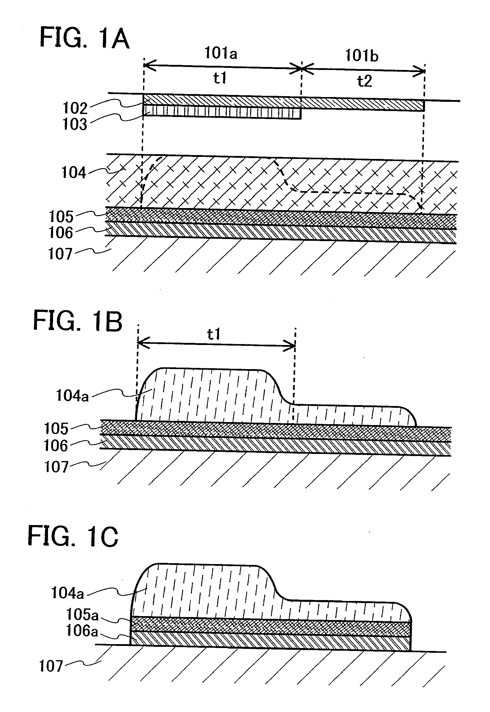
[0088] Description is made of a manufacturing method for forming a reflective electrode and a transparent electrode with reference to FIGS. 1A to 1C and 2A to 2C.
[0089] First, a conductive film 106 is formed over an insulating film 107 by a sputtering method, a printing method, a CVD method, an ink-jet method, or the like. The conductive film 106 may be a transparent conductive film or have a reflecting property. In the case of a transparent conductive film, an indium tin oxide (ITO) film in which tin oxide is mixed in indium oxide, an indium tin silicon oxide (ITSO) film in which silicon oxide is mixed in indium tin oxide (ITO), an indium zinc oxide (IZO) film in which zinc oxide is mixed in indium oxide, a zinc oxide film, a tin oxide film, silicon (Si) containing phosphorus or boron can be used, for example. Note that IZO is a transparent conductive material formed by sputtering using a target in which 2 to 20 wt % of zinc oxide (ZnO) is mixed in ITO; however, a composition rati...
embodiment mode 2
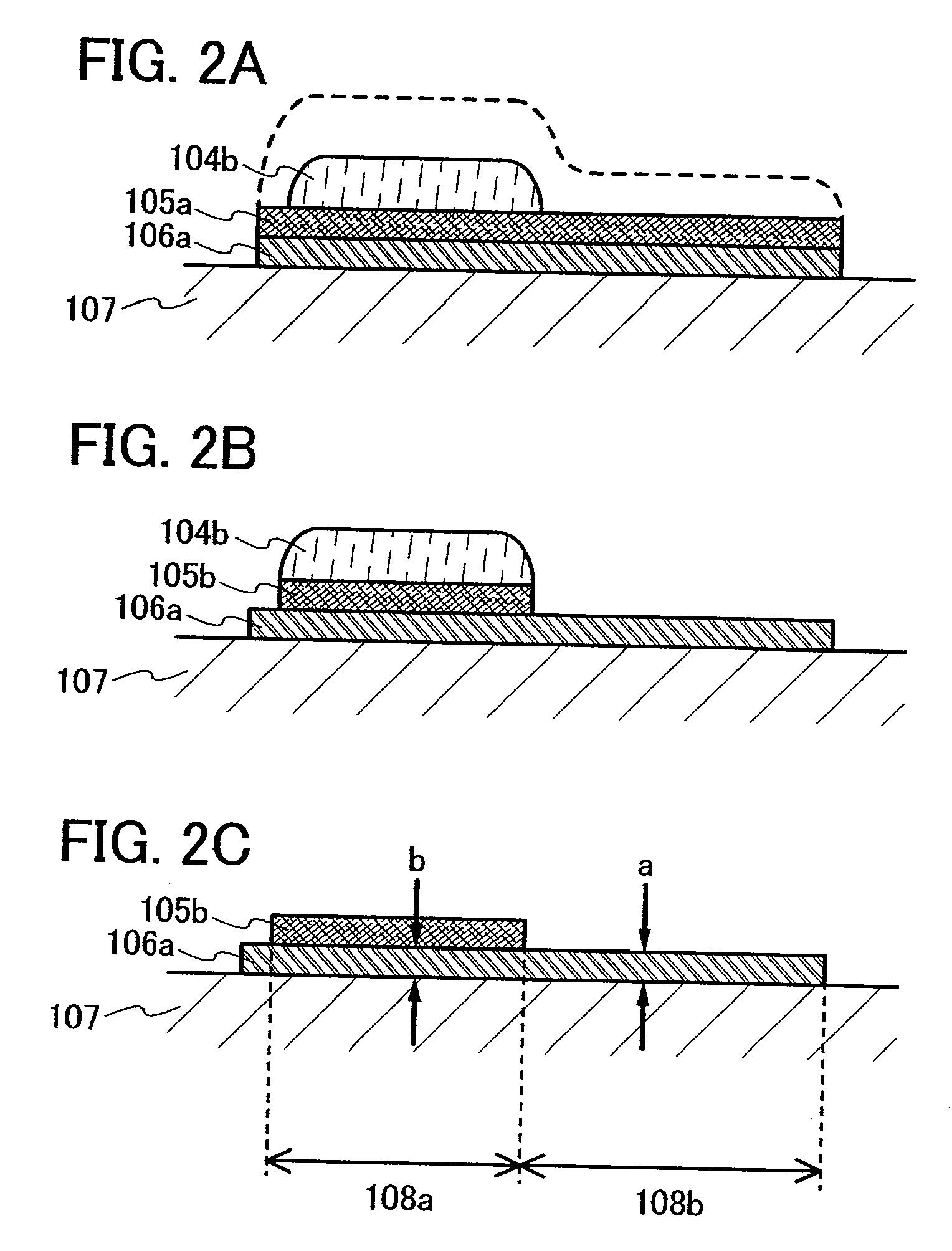
[0122] In Embodiment Mode 1, description is made of the case where a pixel electrode is formed over the insulating film 107. However, actually a pixel electrode is connected to another wiring, transistor, storage capacitor, or the like. Therefore, if required, the insulating film 107 is provided with a contact hole so that the pixel electrode is connected to a wiring or the like.
[0123] Thus, FIG. 4 shows a cross sectional view of that case. An insulating film 107a is provided with a contact hole 402. A wiring 401 is formed below the contact hole 402. The wiring 401 is connected to one of a source or a drain of a transistor in many cases. Alternatively, in many cases, the wiring 401 itself is one of the source or the drain of the transistor, or an electrode of a storage capacitor.
[0124] In this case, the conductive film 106a is required to be formed below the conductive film 105b since the manufacturing method described in Embodiment Mode 1 is used. Therefore, the conductive film 1...
embodiment mode 3
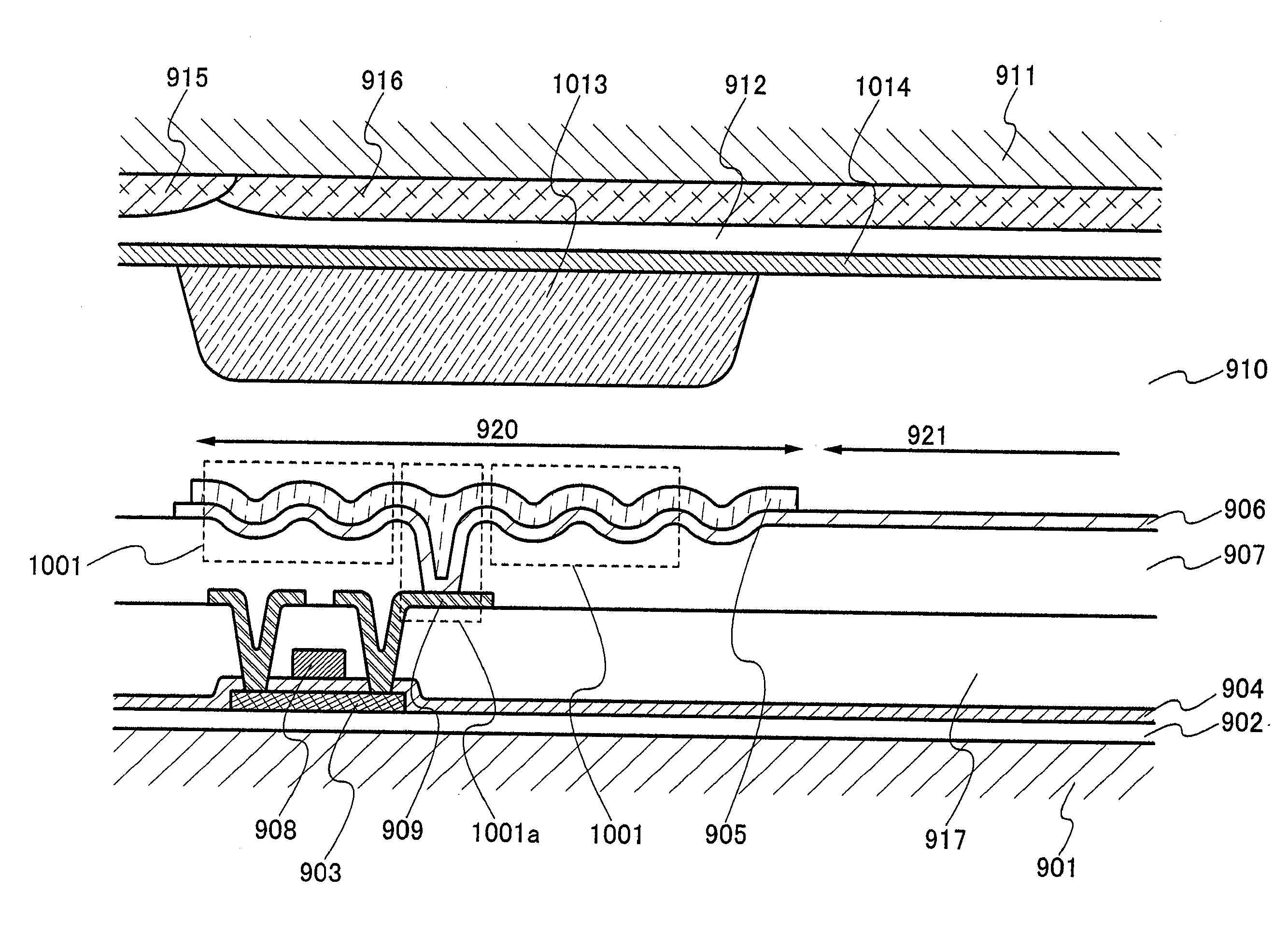
[0141] Next, description is made of a specific example in the case where a transistor is provided. Note that a transistor is not necessarily required and a so-called passive matrix type can also be applied.
[0142] First, description is made of a method for forming a top gate type TFT over a substrate 901 with reference to FIG. 9. The substrate 901 is a substrate having a light transmitting property, such as a quartz substrate, a glass substrate, or a plastic substrate. Note that the substrate 901 may be a substrate having a light shielding property, and a semiconductor substrate or an SOI (Silicon On Insulator) substrate may be used.
[0143] An insulating film 902 is formed over the substrate 901 as a base film. As the insulating film 902, a single layer of an insulating film such as a silicon oxide film, a silicon nitride film, or a silicon oxynitride (SiOxNy) film; or a stacked layer of at least two films of the aforementioned films is used.
[0144] Note that a silicon oxide film is...
PUM
 Abstract
Description
Claims
Application Information