Manufacturing apparatus

a manufacturing apparatus and material technology, applied in the field of manufacturing apparatus, can solve the problems of high cost of fabricating a light emitting device, low and easy difference between film thickness of the center part and the margin of the substrate, so as to promote the efficiency of utilizing expensive el material and improve the uniformity or throughput. the effect of efficiency

Inactive Publication Date: 2007-06-28
SEMICON ENERGY LAB CO LTD
View PDF62 Cites 16 Cited by
  • Summary
  • Abstract
  • Description
  • Claims
  • Application Information

AI Technical Summary

Benefits of technology

[0012] Hence, the present invention provides an evaporation apparatus which is a manufacturing device promoting an efficiency of utilizing an EL material and forming film excellent in uniformity or throughput of forming an EL layer and an evaporation method therefor. Further, the invention provides a light emitting device fabricated by the evaporation apparatus and the evaporation method according to the invention and a method of fabricating the light emitting device.
[0013] Further, the invention provides a manufacturing device of subjecting an EL material to evaporation efficiently to a large area substrate having a substrate size of, for example, 320 mm×400 mm, 370 mm×470 mm, 550 mm×650 mm, 600 mm×720 mm, 680 mm×880 mm, 1000 mm×1200 mm, 1100 mm×1250 mm or 1150 mm×1300 mm. The present invention also provides an evaporation apparatus that can obtain uniform film thickness for a large area substrate in its whole surface.
[0014] Further, the invention provides a fabricating device capable of avoiding an impurity from mixing to an EL material.

Problems solved by technology

Therefore, in forming the EL layer, an efficiency of utilizing the expensive EL material is as extremely low as about 1% or smaller and fabricating cost of a light emitting device becomes very expensive.
Moreover, when the substrate becomes larger, there is the problem that the film thickness of the center part and the margin of the substrate easily become different.
Further, the evaporation apparatus is of a structure of rotating the substrate and therefore, there is a limit in the evaporation apparatus aiming at a large area substrate.
Further, the EL material poses a problem of being deteriorated by being easily oxidized by presence of oxygen or water.
However, in forming a film by an evaporation method, a predetermined amount of an evaporation material put into a vessel (glass bottle) is taken out and transferred to a vessel (representatively, crucible, or evaporation boat) installed at a position opposed to an object to be formed with a film at inside of an evaporation apparatus stem and there is a concern that the evaporation material is mixed with oxygen or water or an impurity in the transferring operation.
However, when the glove is provided at the pretreatment chamber, vacuum cannot be constituted, the operation is carried out under atmospheric pressure and there is a high possibility of mixing an impurity.
For example, even when the transferring operation is carried out at inside of the pretreatment chamber subjected under a nitrogen atmosphere, it is difficult to reduce moisture or oxygen as less as possible.
Further, although it is conceivable to use a robot, since the evaporation material is in a powder-like shape, it is very difficult to fabricate the robot for carrying out the transferring operation.
Therefore, it is difficult to constitute steps of forming an EL element, that is, from a step of forming an EL layer above a lower electrode to a step of forming an upper electrode by an integrated closed system enabling to avoid mixing of an impurity.

Method used


Image

  • Manufacturing apparatus
  • Manufacturing apparatus
  • Manufacturing apparatus

Examples


embodiments

Embodiment 1

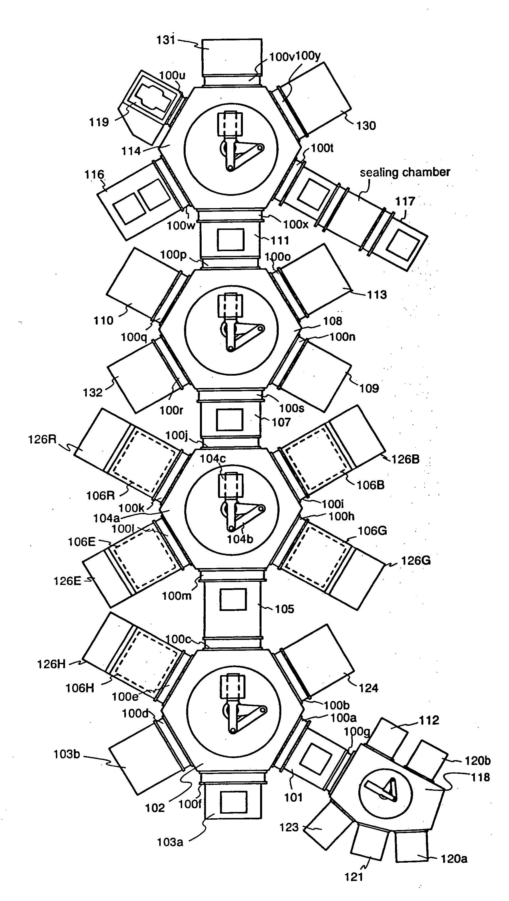
[0126] An example of a multi-chamber manufacturing apparatus in which manufacturing processes from a first electrode up through sealing are automated is shown in FIG. 1 in this embodiment.

[0127]FIG. 1 is a multi-chamber manufacturing apparatus that includes gates 100a to 100y; an extraction chamber 119; transporting chambers 102, 104a, 108, 114, and 118; delivery chambers 105, 107, and 111; a stocking chamber (loading chamber) 101; a first film formation chamber 106H; a second film formation chamber 106B; a third film formation chamber 106G; a fourth film formation chamber 106R; a fifth film formation chamber 106E; other film formation chambers 109 (ITO or IZO film), 110 (a metal film), 112 (spin coat or ink jet), 113 (SiN film or SiOx film), 131 (sputtering chamber), and 132 (sputtering chamber); installation chambers 126R, 126G, 126B, 126E, and 126H for disposing evaporation sources; preprocessing chambers 103a (bake or O2 plasma, H2 plasma, Ar plasma) and 103b (vacu...

embodiment 2

[0160] An example having one portion that differs from the manufacturing apparatus of Embodiment 1 is disclosed in this embodiment. Specifically, an example of a manufacturing apparatus including a transporting chamber 1004a provided with six film formation chambers 1006R (EL layer for red), 1006G (EL layer for green), 1006B (EL layer for blue), 1006R′ (EL layer for red), 1006G′ (EL layer for green), and 1006B′ (EL layer for blue) is shown in FIG. 10.

[0161] Note that portions identical to those of FIG. 1 are shown by using the same reference numerals in FIG. 10. Further, explanations of portions identical to those of FIG. 1 are omitted here for brevity.

[0162] An example of an apparatus capable of manufacturing full color light emitting elements in parallel is shown in FIG. 10.

[0163] Similarly to Embodiment 1, vacuum heating is performed on substrates in the preprocessing chamber 103b, and the substrates are then transported from the transporting chamber 102 to the transporting ch...


PUM

PropertyMeasurementUnit
temperatureaaaaaaaaaa
pressureaaaaaaaaaa
distanceaaaaaaaaaa

Abstract

The present invention provides an evaporation apparatus, which is one type of film formation apparatus and provides superior uniformity in EL layer film thickness, superior throughput, and improved utilization efficiency of EL materials and an evaporation method. The present invention is characterized in that an evaporation source holder, in which a container that encloses an evaporation material is disposed, is moved at a certain pitch with respect to a substrate during evaporation. Further, a film thickness monitor is integrated with the evaporation source holder for the movement. Furthermore, film thickness can be made uniform by adjusting the moving speed of the evaporation source holder in accordance with values measured by the film thickness monitor.

Description

BACKGROUND OF THE INVENTION [0001] 1. Field of the Invention [0002] The present invention relates to a manufacturing method provided with a deposition device for depositing materials which can be deposited by evaporation (hereinafter, an evaporation material), and a manufacturing method of a light emitting device that has a layer containing an organic compound as a light emitting layer with the manufacturing apparatus. Specifically, the present invention relates to a vacuum-evaporation method and an evaporation apparatus that conducts deposition by evaporating an evaporation material from a plurality of evaporation sources provided to face a substrate. [0003] 2. Description of the Related Arts [0004] In recent years, a research related to a light emitting device having an EL element as a self-luminous light emitting element has been activated. The light emitting device is referred to as EL display or light emitting diode (LED). Since these light emitting devices have characteristics...

Claims


Application Information

Patent Timeline
Patent Type & Authority Applications(United States)
IPC IPC(8): C23C16/00C23C14/04H05B33/10C23C14/24C23C14/56H01L21/00H01L51/40H01L51/56
CPCC23C14/042C23C14/243C23C14/568H01L21/67161H01L21/67167H01L51/56H01L21/67236H01L21/67253H01L21/67745H01L51/0004H01L51/001H01L21/67184H10K71/13H10K71/164H10K71/00H05B33/10
Inventor YAMAZAKI, SHUNPEIMURAKAMI, MASAKAZU
Owner SEMICON ENERGY LAB CO LTD
Why Eureka
Try Eureka