Passivating layer for photovoltaic cells

a photovoltaic cell and passivating layer technology, applied in the field of polymer-based electronic devices, can solve the problems of short lifetime of polymer-based devices, increased thickness, and loss of flexibility, and achieve the effect of enhancing the lifetime of photovoltaic cells

Inactive Publication Date: 2007-07-26
RGT UNIV OF CALIFORNIA
View PDF6 Cites 26 Cited by
  • Summary
  • Abstract
  • Description
  • Claims
  • Application Information

AI Technical Summary

Benefits of technology

[0086] A photovoltaic cell is provided comprising a first electrode, a second electrode, a photoactive, charge-separating layer comprising a semiconducting polymer blended with a suitable acceptor between the first and the second ...

Problems solved by technology

Although electronic devices such as diodes, field effect transistors (FETs), light-emitting diodes (LEDs), solar cells, and photodetectors fabricated from semiconducting and metallic polymers have been demonstrated with performance comparable to or in some cases even better than their inorganic counterparts, the typically short lifetime of the polymer-based devices must be overcome before large scale commercialization can be realized.
Photo-oxidation is often a serious problem to polymer-based electronic devices.
Although such encapsulation methods can reduce ...

Method used


Image

  • Passivating layer for photovoltaic cells
  • Passivating layer for photovoltaic cells
  • Passivating layer for photovoltaic cells

Examples


example 1

Solution-Processed Titanium Oxides

[0157] The TiOx material was prepared using a novel sol-gel procedure as follows: 10 mL titanium(IV) isopropoxide (Ti[OCH(CH3)2]4, 99.999%, Sigma-Aldrich Corporation) was mixed with 50 mL 2-methoxyethanol (CH3OCH2CH20H, 99.9+%, Sigma-Aldrich) and 5 mL ethanolamine (H2NCH2CH2OH, 99+%, Sigma-Aldrich) in a three-necked flask equipped with a condenser, thermometer, and an argon gas inlet / outlet respectively. The mixed solution was then heated to 80° C. for 2 hours in a silicon oil bath under magnetic stirring, followed by heating to 120° C. for 1 hour. The two-step heating (at 80° C. and 120° C.) was then repeated. A TiOx precursor solution was prepared in isopropyl alcohol.

[0158] Dense TiOx layers were prepared from the TiOx precursor solution. The precursor solution was spin-cast in the air on top of a semiconducting polymer layer comprising P3HT with thicknesses ranging from 20 to 40 nm. Subsequently, the films were heated at 80° C. for 10 minutes ...

example 2

TiOx as an Oxygen Barrier and an Oxygen Scavenging Layer

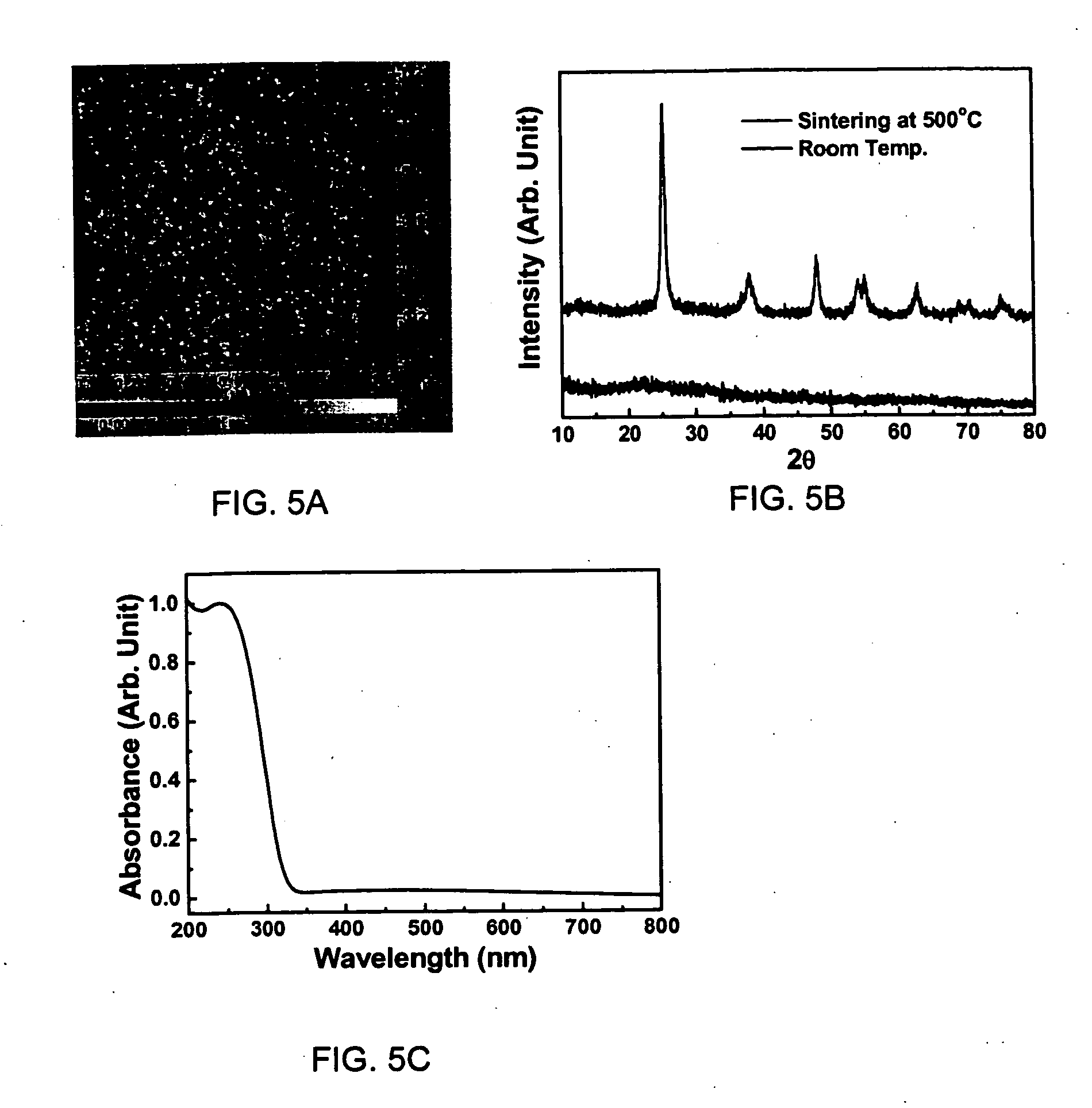
[0161] Comparison studies of photoluminescence (PL) stability of polyfluorene (PF) with and without a TiOx layer were carried out to confirm the oxygen barrier and scavenging properties of the TiOx layer. Four films with the following structures were prepared by spin-casting: glass / PF, glass / TiOx / PF, glass / PF / TiOx, and glass / TiOx / PF / TiOx. The films Were then heated for 15 hours at 150° C. in the air.

[0162] It is known that the PF type materials degrade with an appearance of a long-wavelength emission around 500-600 nm after heating in the air. This green emission peak arises by energy transfer from singlet excitons on the PF chains to keto-defect sites that form by reaction with oxygen present in the luminescent polymer. Therefore, it is expected that the four different samples would exhibit different peak intensities for the long wavelength emission because of the shielding and oxygen scavenging effect of the TiOx layer.

[01...

example 3

Polymer Diodes and Polymer Light-Emitting Diodes with Enhanced Performance as a Result of a Titanium Oxide (TiOx) Layer

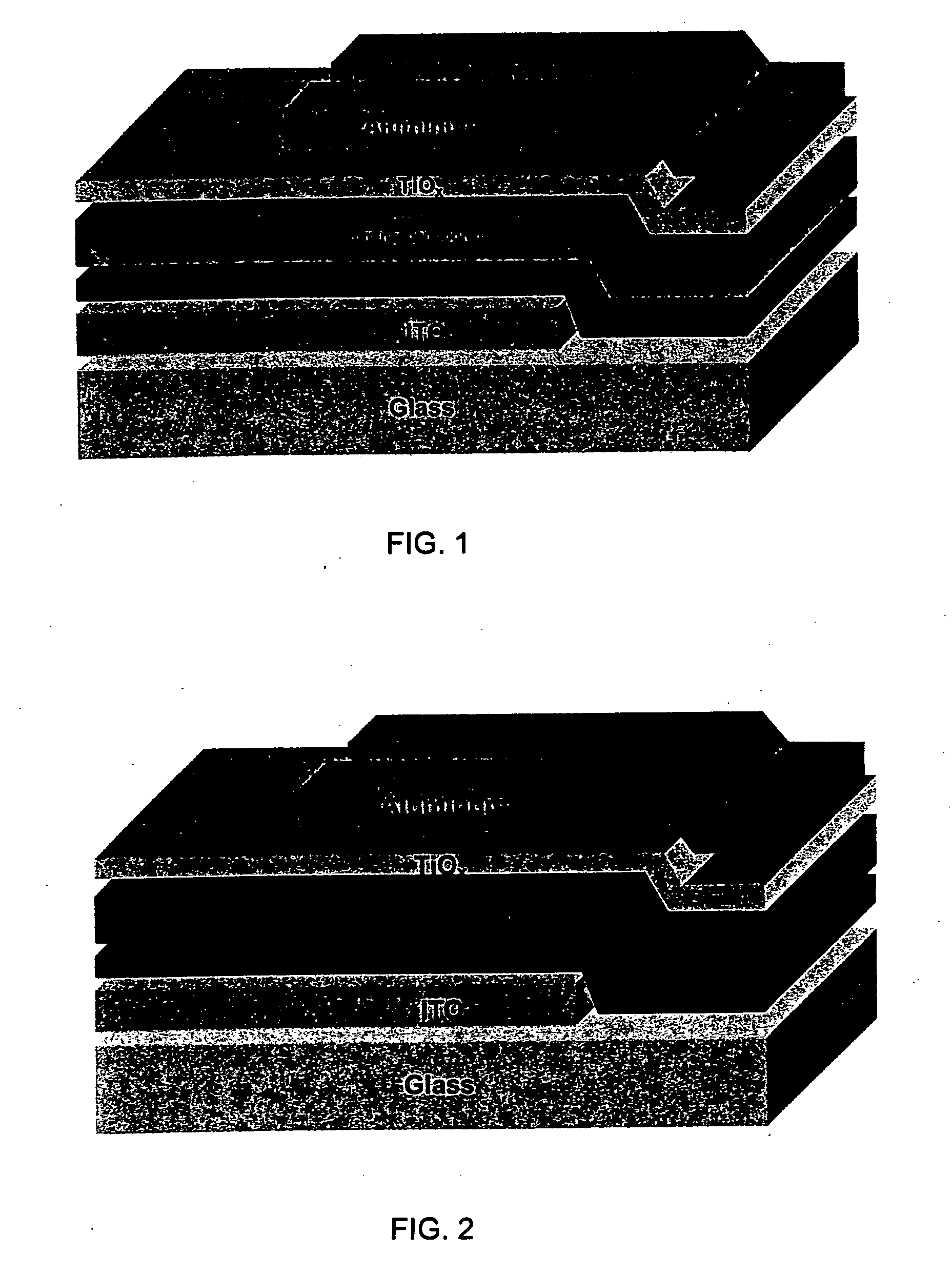
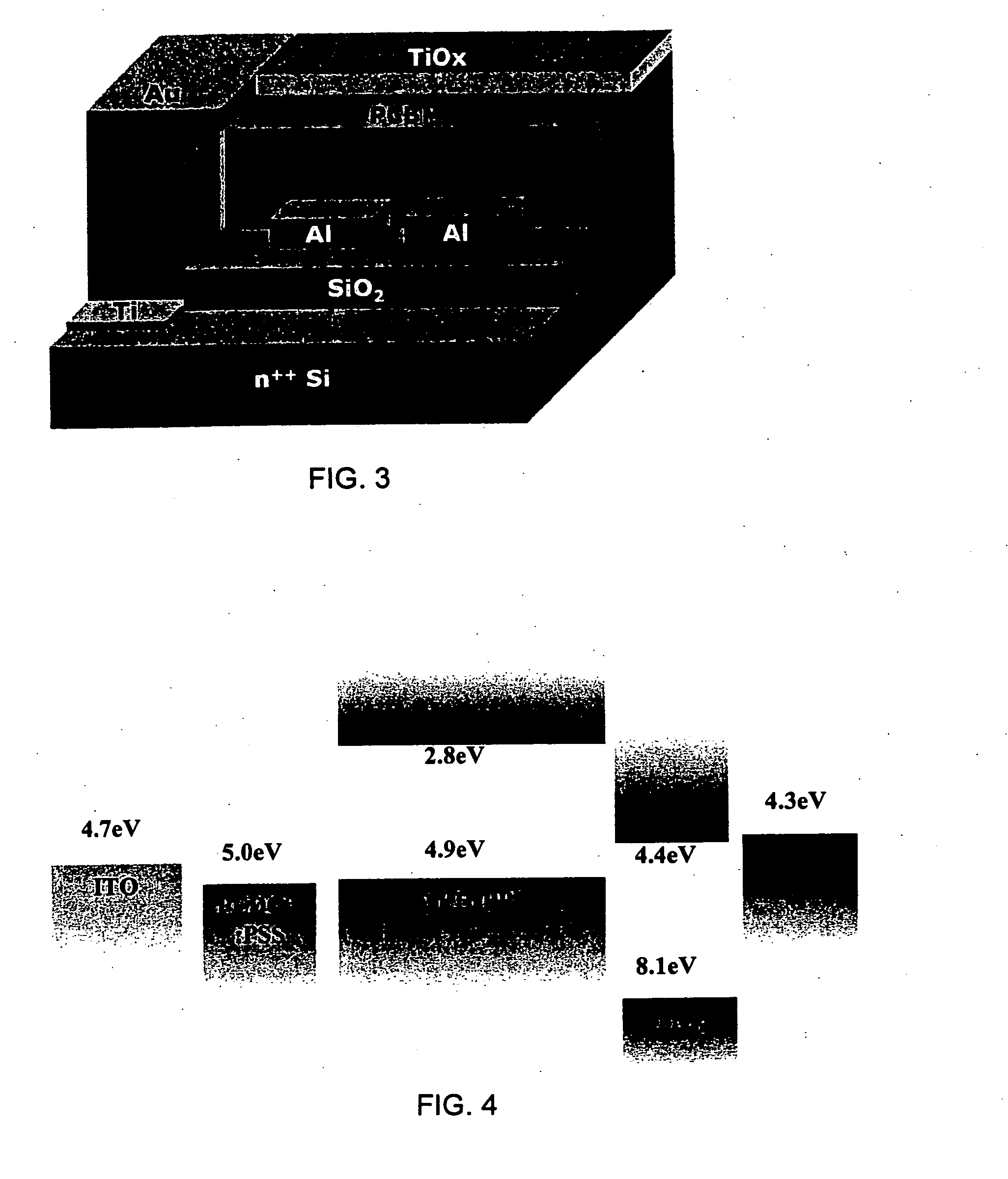
[0166] Polymer diodes and LEDs were fabricated in the sandwich structure: ITO / PEDOT:PSS / Polymer / TiOx / Al. The semiconducting polymer used in this example was MEH-PPV available from Organic Vision Inc. The thickness of the MEH-PPV layer was approximately 100 nm. The TiOx precursor solution (1 wt %) was spin-cast (6000 rpm) onto the semiconducting polymer layer with a thickness around 20 nm, and heated at 80° C. for 10 minutes in the air. During this process the precursor converted to TiOx. Subsequently the devices were pumped down in vacuum (−6 Torr), and then Al electrode with a thickness around 150 nm was deposited. The deposited Al electrode area defined an active area of the device as 16 mm2. The current density-voltage-luminance characteristics were measured using a Keithley 236 source measurement unit along with a calibrated silicon photodiode inside a glove bo...


PUM

PropertyMeasurementUnit
Temperatureaaaaaaaaaa

Abstract

A photovoltaic cell which comprises a first electrode, a second electrode, a photoactive, charge-separating layer comprising a semiconducting polymer between the first and the second electrodes, and a passivatng layer adapted to enhance the lifetime of the photovoltaic cell. The passivating layer comprises a substantially amorphous titanium oxide having the formula of TiOx where x represents a number from 1 to 1.96.

Description

CROSS-REFERENCE TO RELATED APPLICATIONS [0001] This application is a continuation-in-part of U.S. patent application Ser. No. 11 / 347,111 filed Feb. 2, 2006, which claims the benefit of priority under 35 USC § 119(e) to U.S. Provisional Patent Application Ser. No. 60 / 663,398 filed Mar. 17, 2005, and which is a continuation-in-part of U.S. patent application Ser. No. 11 / 326,130 filed Jan. 4, 2006, which in turn claims the benefit of priority under 35 USC § 119(e) to U.S. Provisional Patent Application Ser. No. 60 / 663,398 filed Mar. 17, 2005, the disclosures of all of which are incorporated herein by reference in their entirety. This Application claims the benefit of priority under 35 USC § 119(e) to U.S. Provisional Application Ser. Nos. 60 / 756,604 filed Jan. 4, 2006, and 60 / 872,401 filed Feb. 1, 2006, the disclosures of which are incorporated herein by reference in their entirety.BACKGROUND [0002] This invention relates generally to polymer-based electronic devices and in particular ...

Claims


Application Information

Patent Timeline
IPC IPC(8): H01L31/00H01L21/00H01L51/40
CPCB82Y10/00H01L51/0036H01L51/0037H01L51/0047Y02E10/549H01L51/4253H01L51/441H01L51/448H01L2251/308H01L51/4226H10K85/113H10K85/1135H10K85/215H10K30/151H10K30/30H10K30/81H10K30/88H10K2102/103H10K30/50
Inventor LEE, KWANGHEEHEEGER, ALAN J.
Owner RGT UNIV OF CALIFORNIA
Why Eureka
Try Eureka