Method and system for high-speed precise laser trimming and scan lens for use therein

a laser and scanning lens technology, applied in the field of laser material processing, can solve the problems of reducing resistance drift, out of specifications, nothing gained, etc., and achieve the effect of improving post-cut stability and precise trimming

Inactive Publication Date: 2007-08-02
ELECTRO SCI IND INC
View PDF92 Cites 25 Cited by
  • Summary
  • Abstract
  • Description
  • Claims
  • Application Information

AI Technical Summary

Benefits of technology

[0017] An object of the present invention is to provide an improved method and system for high-speed, precise trimming utilizing a laser and scan lens for use therein wherein post trim stability is improved.
[0018] In carrying out the above object and other objects of the present invention, a method is provided for high-speed, laser-based, precise laser trimming at least one electrical element. Each electrical element has at least one measurable property and is supported on a substrate. The method includes generating a pulsed laser output with a laser, the output has one or more laser pulses at a repetition rate. Each laser pulse has a pulse energy, a laser wavelength within a range of laser wavelengths, and a pulse duration. The method further includes selectively irradiating the at least one electrical element with the one or more laser pulses focused into at least one spot having a non-uniform intensity profile along a direction and a spot diameter less than about 15 microns so as to cause the one or more laser pulses having the wavelength, energy, pulse duration and the spot diameter to selectively remove material from the at least one element along a trim path and laser trim the at least one element while avoiding substantial microcracking within the at least one element. The wavelength is short enough to produce desired short-wavelength benefits of small spot size, tight tolerance, high absorption and reduced or eliminated heat-affected zone (HAZ) along the trim path, but not so short so as to cause microcracking.
[0019] The focused pulsed laser output power may correspond to about 10-50 mw with a spot diameter of less than about 15 μm. The power is scalable with reduced spot sizes less than about 15 μm such that corresponding power density is high enough to trim the element but sufficiently low to avoid microcracking.

Problems solved by technology

One of the challenges is always to reduce the resistance drift after the trimming process.
If the device later drifts out of specifications, nothing has been gained.
It has been known that trim induced instability or long-term drift arises from the heat-affected zone (HAZ) along the laser cut edges and any residual material in the cut itself.
The laser trim itself causes heating and melting of film material near the trim.
With the current laser technology, this potential instability due to the heat-affected zone along the laser cut edges remains.
This is inherent in the trim process and it cannot be eliminated.
But links with reasonable resolution require a disproportionate share of the device real estate and are only used for simple trims such as op-amp offset voltage or in conjunction with a continuous trim in a course / fine arrangement.
However, this will squander precious real estate since cutting drift in half requires doubling the resistor size.
This is limited, however, by the choice of the laser wavelength, of optics, and by various practicalities such as reduced depth of focus, less working distance, and material re-deposition in the case of thick films.
However, considering increased lens aberrations and manufacturing tolerances, this may not be achievable.

Method used


Image

  • Method and system for high-speed precise laser trimming and scan lens for use therein
  • Method and system for high-speed precise laser trimming and scan lens for use therein
  • Method and system for high-speed precise laser trimming and scan lens for use therein

Examples


Embodiment Construction

)

High-Speed Serpentine Trimming Process

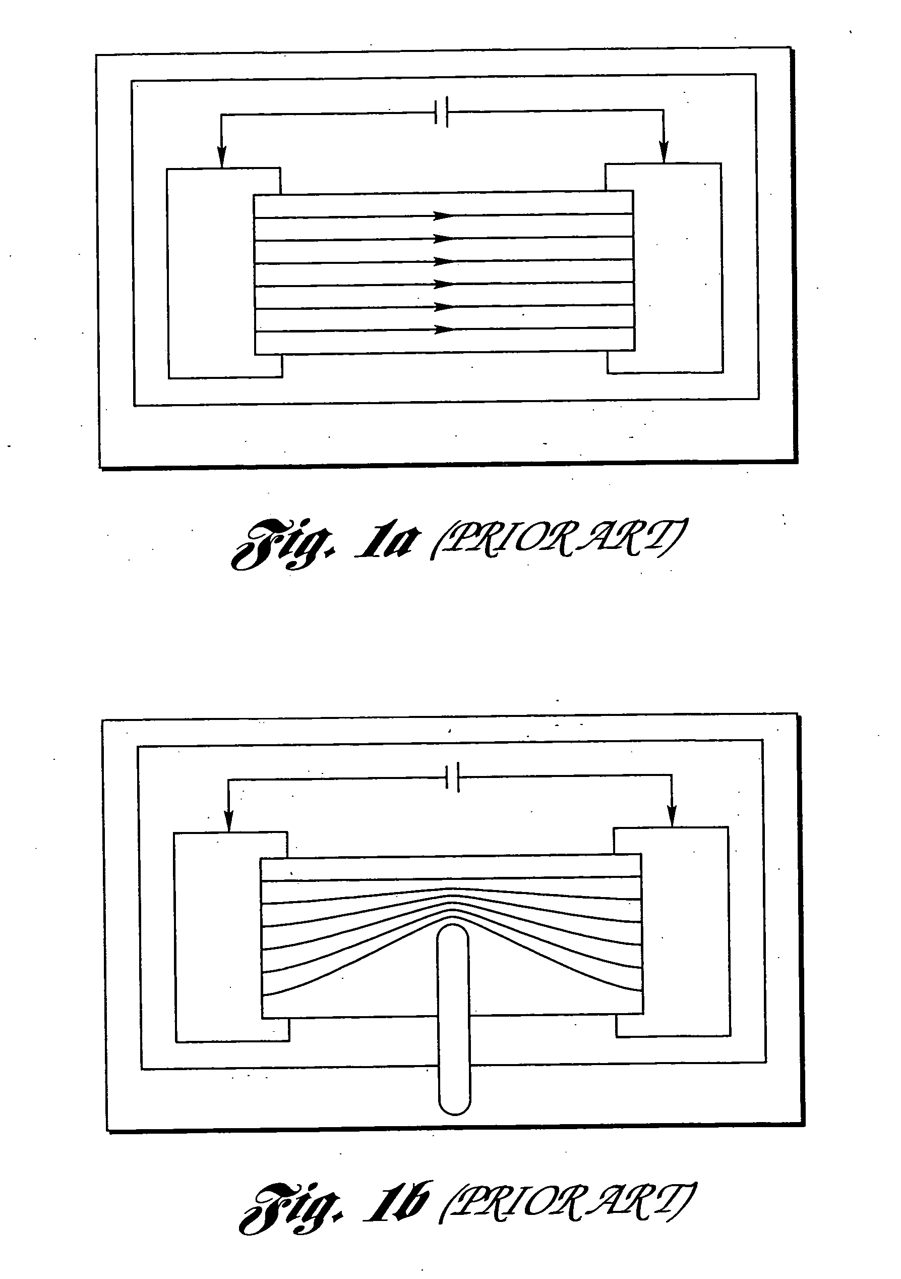
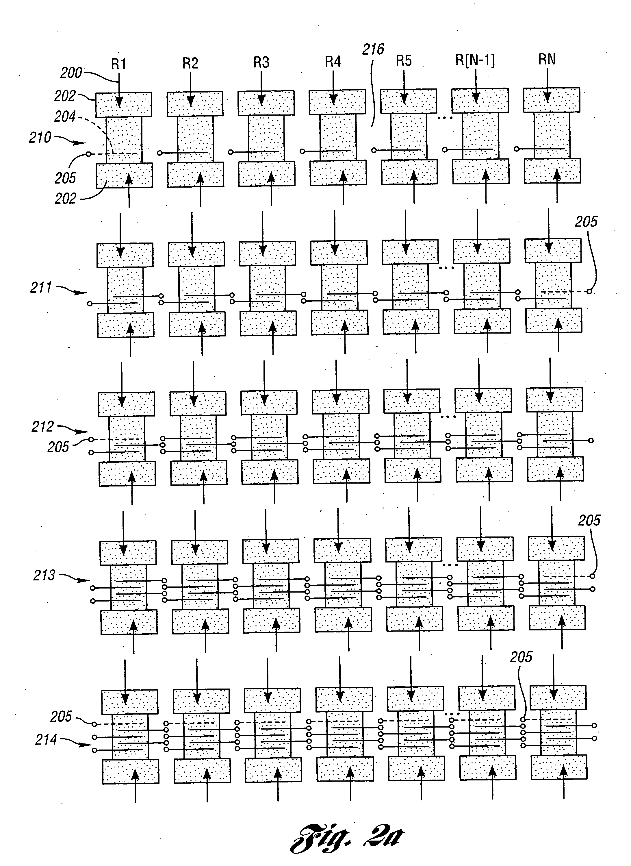
[0092] In resistor trimming, the cuts direct the current flowing through the resistive material along a resistance path. Fine control and adjustment of the cut size and shape change the resistance to a desired value, as illustrated in FIGS. 1a-1c. Typically, chip resistors are arranged in rows and columns on a substrate. FIG. 2a shows an arrangement wherein a row of resistors R1,R2, . . . RN is to be processed. A probe array, having a probe 200 and depicted by arrows in FIG. 2a, is brought into contact 202 with the conductors of a row of resistors. A matrix switch addresses the contacts for a first pair of conductors (e.g.: contacts across R1) and a series of cuts and measurements is performed to change the resistance between the conductor pair to a desired value. When the trimming of a resistor is complete, the matrix switches to a second set of contacts at the next row element (e.g.: R2) and the trimming process is repeated. When a complete...


PUM

PropertyMeasurementUnit
diameteraaaaaaaaaa
diameteraaaaaaaaaa
visible wavelength rangeaaaaaaaaaa

Abstract

A method, system and scan lens for use therein are provided for high-speed, laser-based, precise laser trimming at least one electrical element along a trim path. The method includes generating a pulsed laser output with a laser, the output having one or more laser pulses at a repetition rate. A fast rise / fall time, pulse-shaped q-switched laser or an ultra-fast laser may be used. Beam shaping optics may be used to generate a flat-top beam profile. Each laser pulse has a pulse energy, a laser wavelength within a range of laser wavelengths, and a pulse duration. The wavelength is short enough to produce desired short-wavelength benefits of small spot size, tight tolerance, high absorption and reduced or eliminated heat-affected zone (HAZ) along the trim path, but not so short so as to cause microcracking. In this way, resistance drift after the trimming process is reduced.

Description

CROSS-REFERENCE TO RELATED APPLICATIONS [0001] This application claims the benefit of U.S. Provisional Application Ser. No. 60 / 763,242, filed Jan. 30, 2006, entitled “Method and System for High-Speed Precise Laser Trimming, Scan Lens System for Use Therein and Electrical Device Produced Thereby.” This application claims priority to and is a continuation-in-part of U.S. patent application Ser. No. 11 / 376,527, filed Mar. 15, 2006, entitled “Method and System for High-Speed Precise Laser Trimming and Electrical Device Produced Thereby.” That application claims priority to and is a continuation-in-part application of U.S. patent application Ser. No. 11 / 245,282, filed Oct. 6, 2005. That application claims the benefit of U.S. provisional application Ser. No. 60 / 617,130, filed Oct. 8, 2004, entitled “Laser System And Method For Laser Trimming.” This application also claims priority to and is a continuation-in-part application of U.S. patent application Ser. No. 11 / 131,668, entitled “Method...

Claims


Application Information

Patent Timeline
Patent Type & Authority Applications(United States)
IPC IPC(8): H01L21/00B23K26/38
CPCB23K26/0003H01C17/242B23K26/365B23K26/063B23K26/0622B23K26/351B23K26/361
Inventor GU, BOEHRMANN, JONATHAN S.LENTO, JOSEPH V.COUCH, BRUCE L.CHU, YUN FEEJOHNSON, SHEPARD D.
Owner ELECTRO SCI IND INC
Why Eureka
Try Eureka