Intercalated superlattice compositions and related methods for modulating dielectric property

a superlattice composition and intercalation technology, applied in the direction of thin material processing, material nanotechnology, coatings, etc., can solve the problems of prohibitively excessive power consumption, semiconductor carrier mobility, and art remains somewhat lacking, so as to simplify device design and performance enhancement, increase the dielectric and/or capacitance properties of self-assembled organic components, and improve the k value of the dielectric composition

Active Publication Date: 2007-08-09
NORTHWESTERN UNIV
View PDF1 Cites 84 Cited by
  • Summary
  • Abstract
  • Description
  • Claims
  • Application Information

AI Technical Summary

Benefits of technology

[0009] It can be an object of the present invention to provide an organic insulator material to reduce operating voltage in TFT and related device structures. In conjunction therewith, it can be another object of the present invention to provide such a material composition which increases the drain current of such a device while operating at low biases. Relating to one or more of the preceding objectives, it can also be an object of this invention to achieve such results by increasing the capacitance of a gate dielectric material.
[0021] A component-by-component, layer-by-layer modularity can provide for incorporation or intercalation of other structural and / or functional (e.g., optical, magnetic, mechanical) components or constituents during assembly. In accordance therewith and as described below, the dielectric and / or capacitance properties of a self-assembled organic component can be increased beyond what is possible for such organic materials of the prior art, thereby enabling simplified device design and performance enhancement. Accordingly, the present invention can also be directed to incorporation or intercalation of a metal / metal oxide component imparting or contributing a high k value to the resulting dielectric composition. In certain embodiments, and as described elsewhere herein, such incorporation can be achieved by depositing such a component or precursor thereto on an aforementioned siloxane moiety. However, as would be understood by those skilled in the art made aware of this invention, such components could be otherwise intercalated, substantially without adverse impact on the dielectric properties of such structures.
[0026] As demonstrated below, intercalation of one or more metal oxide layers, employing one or more of a variety of metal oxides, into self-assembled superlattices (SASs) can efficiently modulate the dielectric properties of a SAS dielectric, and the resulting films can be easily integrated into OTFT devices. The results support application of this invention not only in OFET technologies but also as capacitative elements in LC displays, supercapacitors, and other insulated field-effect devices.

Problems solved by technology

While carrier mobilities of organic semiconductors have now approached / surpassed those of amorphous Si, this has generally been achieved only at very large source-drain / source-gate biases, typically greater than 30-50 V. OTFT operation at such large biases will incur prohibitively excessive power consumption.
Further, in such devices, the semiconductor carrier mobility is gate bias dependent and increases when the gate voltage is increased.
Notwithstanding such concerns, the art remains somewhat lacking and the search continues for viable alternatives to SiO2 insulator materials.

Method used


Image

  • Intercalated superlattice compositions and related methods for modulating dielectric property
  • Intercalated superlattice compositions and related methods for modulating dielectric property
  • Intercalated superlattice compositions and related methods for modulating dielectric property

Examples


example 1

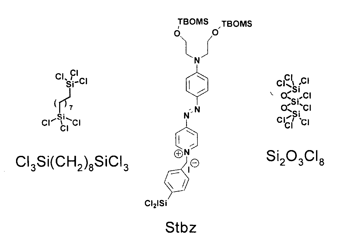
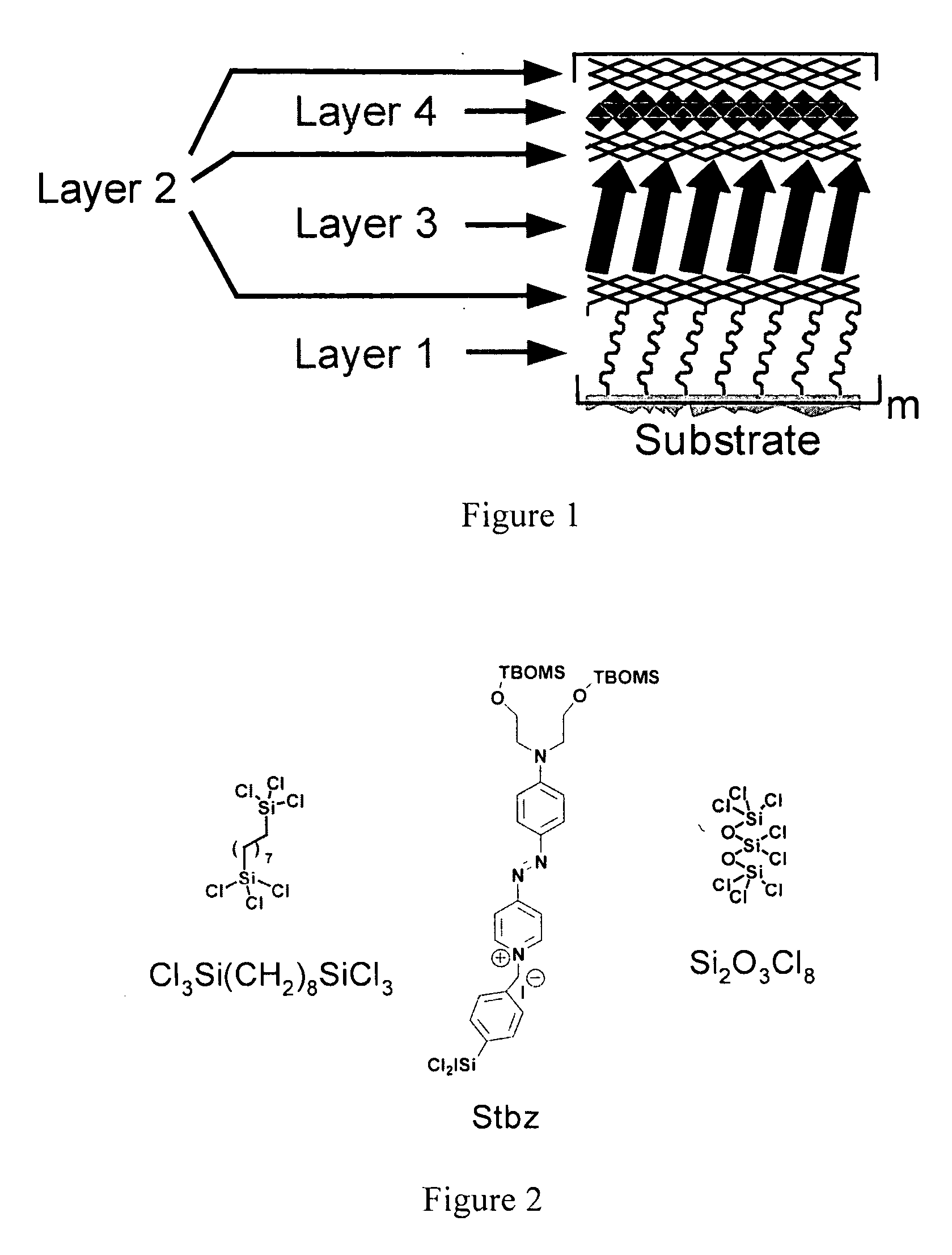
[0051] Materials. The Cl3Si(CH2)8SiCl3, octachlorotrisiloxane, and metal alkoxide reagents are commercially available, whereas the Stbz stilbazonium precursor was prepared according to the literature. Native oxide coated highly n-doped silicon (100) wafers were purchased from Montco Silicon Tech, Spring City, Pa. ITO-coated glass substrates (20 U / sq; 20-30-Å rms roughness) were purchased from Donnelly Corp and cleaned according to known procedures [P. Zhu et al., Chem. Mater. 14, 4982 (2002)]. Pentacene was purchased from Aldrich and purified by gradient vacuum sublimation before use. All self-assembly procedures were performed in an N2-filled glove bag. Structures of reagents useful in such self-assembly process as shown in FIG. 2. Various other reagents and component precursors are found in the aforementioned references.

example 2

[0052] Growth of SAS dielectrics. With reference to FIG. 1: Layer 1. Silicon or ITO substrates were loaded into a Teflon sample holder and immersed in a 5 mM toluene solution of Cl3Si(CH2)8SiCl3 at 0 C; after 1 h the substrates were rinsed twice with toluene and then sonicated in acetone-H2O (95-5 v:v) solution for 3 min. The substrates were then dried at 115° C. for 5 min. Layer 2. The substrates were immersed in a dry pentane solution of Si3O2Cl8 (34 mM) for 30 min, washed twice with dry pentane, sonicated in acetone for 15 min, and dried at 115° C. for 5 min. Layer 3. The substrates were immersed in a dry THF solution of Stbz chromophore precursor shown (1-2 mM) for ≧15 min at 60° C. After cooling to 25° C., the substrates were washed with toluene and THF, sonicated in acetone for 5 min., and dried at 115° C. for 5 min. Layer 4. The substrates were immersed in a freshly prepared dry THF solution of metal alkoxide (M=Ti, Zr, Hf; 1.0 mM) for 1-2 h, washed twice with dry THF, washed...

example 3

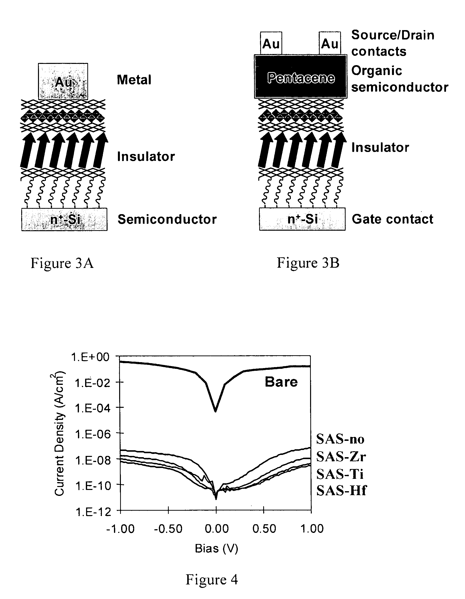
[0053] Device fabrication. For OTFTs, pentacene was vacuum deposited at ˜2×10⁻⁶ Torr (500 Å, 0.2 Å / s) while maintaining the substrate-nanodielectric temperature at 60° C. Gold electrodes for OTFT / MIS devices were vacuum-deposited through shadow masks at 3-4×10⁻⁶ Torr (500-1000 Å, 0.5 Å / s).


PUM


Abstract

Compositions, methods of using inorganic moieties for dielectric modulation, and related device structures.

Description

[0001] This application claims priority benefit from application Ser. No. 60 / 751,861 filed Dec. 20, 2005, the entirety of which is incorporated herein by reference.[0002] The United States government has certain rights to this invention pursuant to Grant No. N00014-05-1-0541 from the Office of Naval Research and Grant No. 521-0077-050-A1 / NCC2-1363 from the National Aeronautics and Space Administration, both to Northwestern University.[0003] The possibility of using small molecules and polymeric organic materials for applications in the electronic / semiconductor industry has been of great scientific and technological interest for several decades. Among the types of organic materials actively investigated have been conducting polymers for charge transporting (contact / electrodes) applications and as sensors / actuators, semiconductors as active components in field-effect / p-n devices, light emitters, laser emitters, energy conversion devices, sensors, and dielectric materials for capacitor...

Claims


Application Information

Patent Timeline
Patent Type & Authority Applications(United States)
IPC IPC(8): B05D1/36H01L29/94H01L21/336
CPCB82Y30/00H01L51/052H01L51/0579H01L51/0533H01L51/0545H01L51/0529Y10T428/31663Y10T428/31536H10K10/471H10K10/474H10K10/476H10K10/466H10K10/23
Inventor MARKS, TOBIN J.FACCHETTI, ANTONIO
Owner NORTHWESTERN UNIV
Why Eureka
Try Eureka