Method of making a thermally treated coated article with transparent conductive oxide (TCO) coating for use in a semiconductor device

a technology of transparent conductive oxide and coating, which is applied in the direction of vacuum evaporation coating, coating, semiconductor devices, etc., can solve the problems of reducing the ability of species, and requiring such high glass substrate temperatures, so as to reduce the fermi level, prevent or reduce the formation of compensating, and reduce the mobility of atoms

Inactive Publication Date: 2007-08-09
GUARDIAN GLASS LLC
View PDF28 Cites 49 Cited by
  • Summary
  • Abstract
  • Description
  • Claims
  • Application Information

AI Technical Summary

Benefits of technology

[0011] In other example embodiments of this invention, the thin film as originally sputter-deposited on the glass substrate may be of or include a zinc oxide based film including Al as a primary dopant and Ag as a co-dopant. The use of both the primary dopant (e.g., Al or the like) and the co-dopant (e.g., Ag or the like) in depositing (e.g., sputter-depositing) the substantially amorphous thin film prevents or reduces the formation of compensating native defects in a wide-bandgap semiconductor material during the impurity introduction by controlling the Fermi level at or proximate the edge of the growth. After being captured by surface forces, atoms start to migrate and follow the charge neutrality principle. The Fermi level is lowered at the growth edge by the addition of a small amount of acceptor impurity (such as Ag) so it prevents or reduces the formation of the compensating (e.g., negative in this case) species, such as zinc vacancies. After the initial stage of the semiconductor layer formation, the mobility of atoms is reduced and the probability of the point defect formation is primarily determined by the respective energy gain. Silver atoms for example in this particular example case tend to occupy interstitial sites where they play a role of predominantly neutral centers, forcing Al atoms to the preferable zinc substitutional sites, where Al plays the desired role of shallow donors, thus eventually raising the Fermi level. In addition, the provision of the co-dopant promotes declustering of the primary dopant, thereby freeing up space in the metal sublattice and permitting more A

Problems solved by technology

Such methods include chemical pyrolysis where precursors are sprayed onto the glass substrate at approximately 400 to 600 degrees C., and vacuum deposition where the glass substrate is kept at about 100 to 300 degrees C. It is often not desirable to require such high glass substrate temperatures for TCO deposition processing.
However, a problem associated with low-temperature sputter deposition is the low atom mobility of the resulting layer on the glass substrate.
This limits the ability of species to find their optimal positions, thereby reducing film quality due to less than desirable crystallinity.
The low atom mobility is particularly problematic for dopant atoms which are often introduced to a stoichiometric film to produce free electrons.
At low deposition temperatures, the dopant atoms tend to cluster such that their efficiency becomes reduced.
Thus, low-temperature sputtering of TCOs has not heretofore been practical.
As mentioned above, typical methods for forming TCO films on glass include chemical pyrolysis where precursor

Method used


Image

  • Method of making a thermally treated coated article with transparent conductive oxide (TCO) coating for use in a semiconductor device
  • Method of making a thermally treated coated article with transparent conductive oxide (TCO) coating for use in a semiconductor device
  • Method of making a thermally treated coated article with transparent conductive oxide (TCO) coating for use in a semiconductor device

Examples


Embodiment Construction

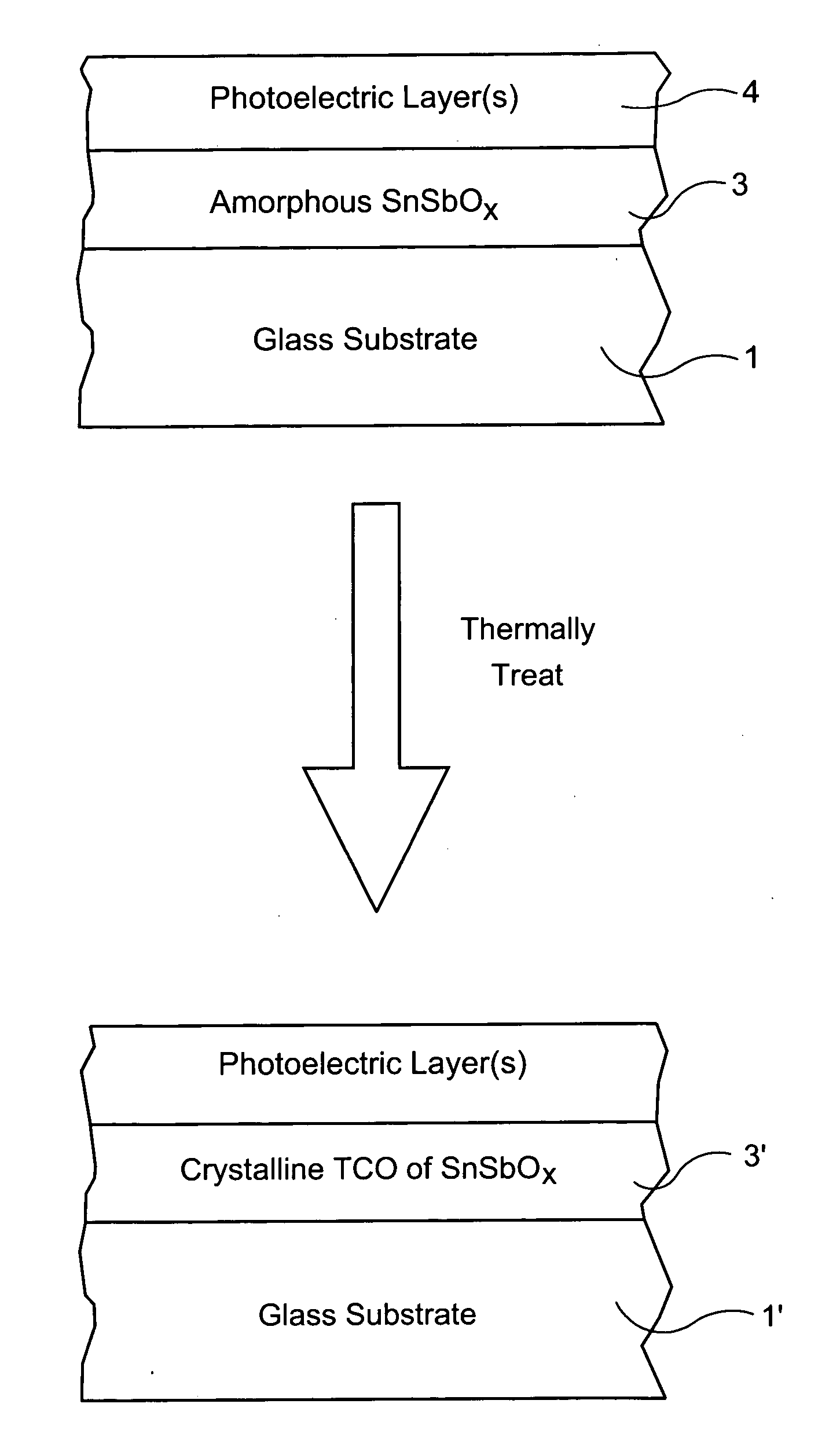
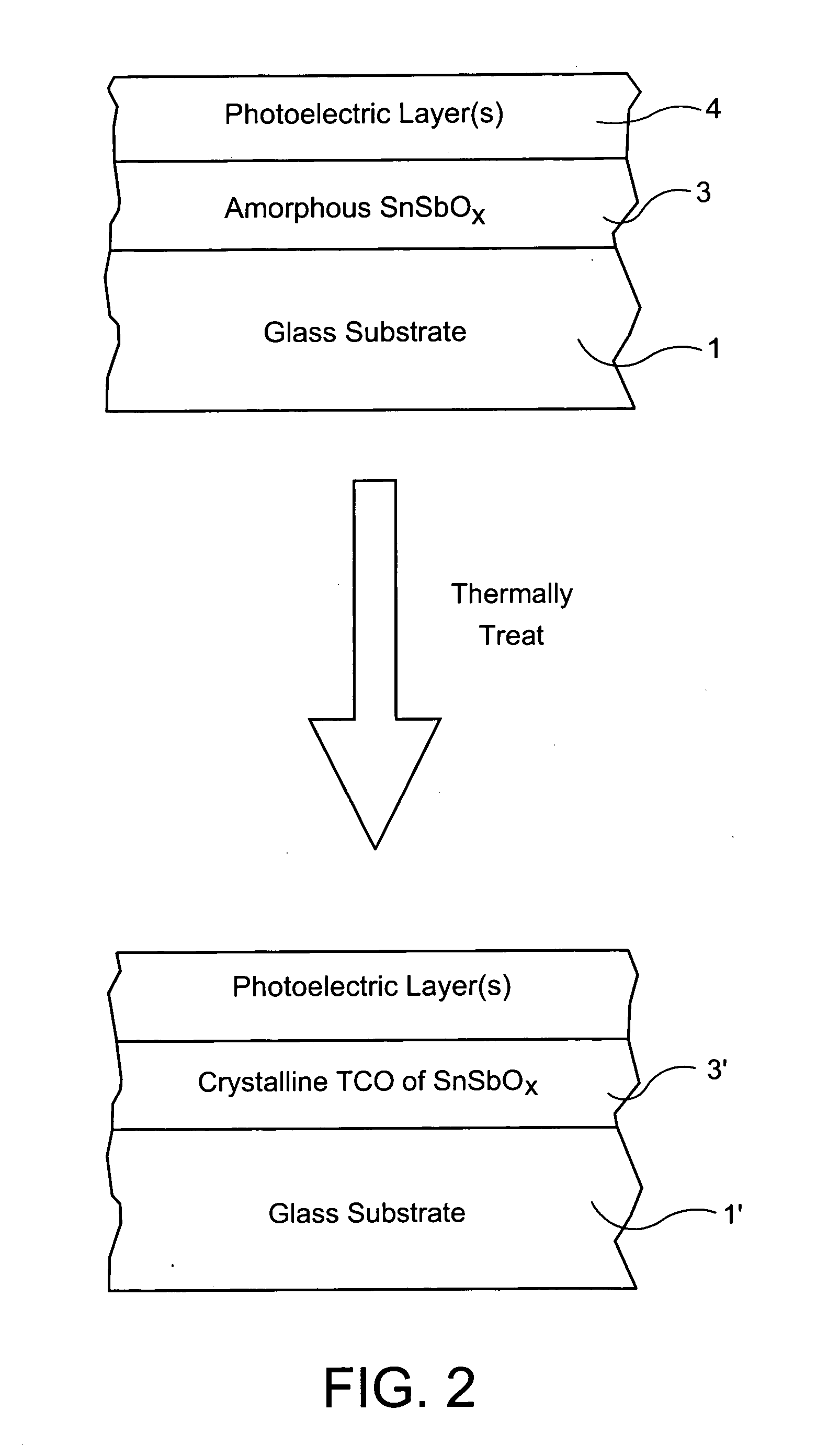
[0016] Coated articles including conductive layer(s) according to certain example non-limiting embodiments of this invention may be used in applications including semiconductor devices such as photovoltaic devices, and / or in other applications such as oven doors, defrosting windows, display applications, or other types of windows in certain example instances. For example and without limitation, the transparent conductive oxide (TCO) layers discussed herein may be used as electrodes in solar cells, as heating layers in defrosting windows, as solar control layers in windows, and / or the like. For example, the TCO film may be used as a front electrode or front contact in a photovoltaic device in certain example instances.

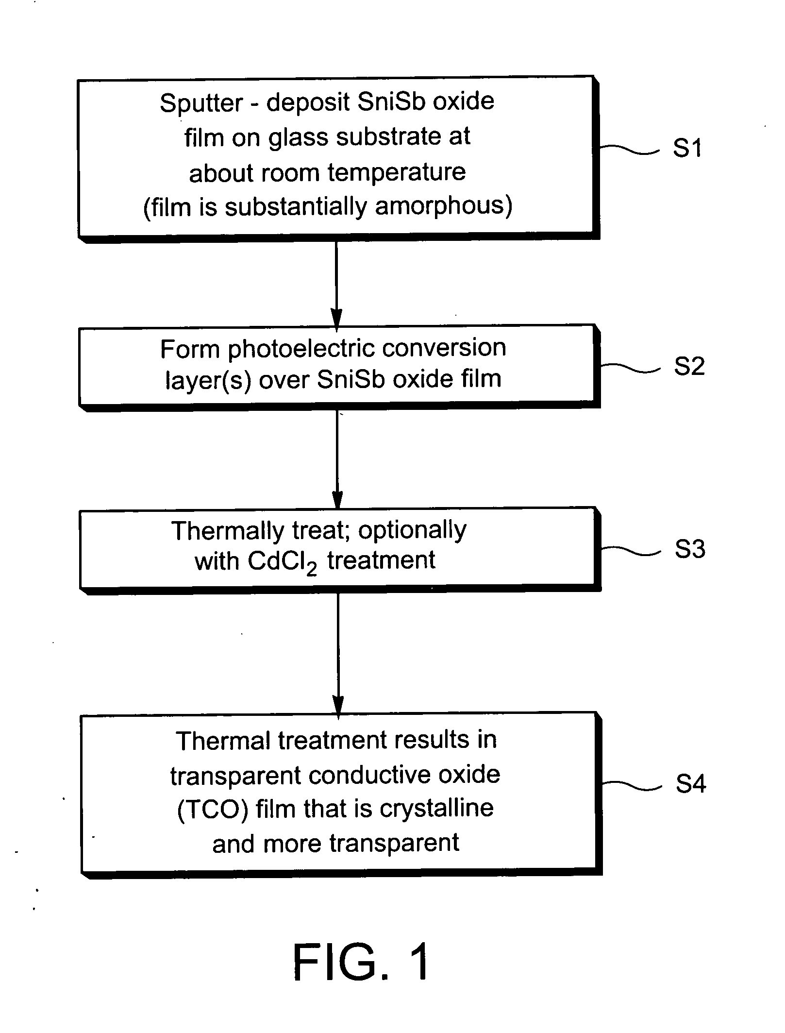
[0017]FIG. 1 is a flowchart illustrating certain steps performed in making a coated article according for use in a semiconductor device according to an example embodiment of this invention, whereas FIG. 2 illustrates this example embodiment in terms of a cross sectiona...


PUM

PropertyMeasurementUnit
Fractionaaaaaaaaaa
Fractionaaaaaaaaaa
Transparencyaaaaaaaaaa

Abstract

A method of making a coated article including a transparent conductive oxide (TCO) film supported by a glass substrate is provided. Initially, an amorphous metal oxide film is sputter-deposited onto a glass substrate, either directly or indirectly. The glass substrate with the amorphous film and a semiconductor film thereon is then thermally treated at high temperature(s). The thermal treating causes the amorphous film to be transformed into a crystalline transparent conductive oxide (TCO) film. The heat used in the thermal treating causes the amorphous film to turn into a crystalline film, causes the visible transmission of the film to increase, and/or causes the film to become electrically conductive.

Description

[0001] This invention relates to a method of making a thermally treated coated article including a transparent conductive oxide (TCO) film supported by a glass substrate. Coated articles according to certain example non-limiting embodiments of this invention may be used in semiconductor applications including photovoltaic devices such as solar cells, or in other applications such as oven doors, defrosting windows, or other types of windows in certain example instances. BACKGROUND AND SUMMARY OF EXAMPLE EMBODIMENTS OF INVENTION [0002] Conventional methods of forming TCOs on glass substrates require high glass substrate temperatures. Such methods include chemical pyrolysis where precursors are sprayed onto the glass substrate at approximately 400 to 600 degrees C., and vacuum deposition where the glass substrate is kept at about 100 to 300 degrees C. It is often not desirable to require such high glass substrate temperatures for TCO deposition processing. [0003] Sputter deposition of ...

Claims


Application Information

Patent Timeline
IPC IPC(8): H01L21/44
CPCC03C17/245C03C17/3429C03C17/3464C03C2217/211C03C2217/216Y02E10/50C03C2217/256C03C2218/154C23C14/086C23C14/5806H01L31/1884C03C2217/244
Inventor KRASNOV, ALEXEY
Owner GUARDIAN GLASS LLC
Why Eureka
Try Eureka