
Eureka
For R&D, Eureka makes reading and utilizing patents & technical documents easy.
Eureka AIR
Designed for self-driven R&D workflows. Generate viable solutions, solve complex R&D challenges, empower your innovation with AI.

Eureka Materials
Designed for material experts only. Revolutionize your material R&D, from search, analyze, to developing new materials.

TechResearch
Generate reliable direction feasibility study reports for your R&D in just a few steps.

TechSeek
Discover and master advanced knowledge NOW. Basics, ideas, possibilities, all at once.

TechMind
As an expert in R&D Theories, TechMind can generates customized viable solutions instantly.

TechRisk
Analyze your overall solution with one click, know your potential R&D risks in advance.

TechMonitor
Get weekly tech updates, stay abreast of the latest tech innovations and key insights.
Materials containing voids with void size controlled on the nanometer scale
- Summary
- Abstract
- Description
- Claims
- Application Information
AI Technical Summary
Benefits of technology
Problems solved by technology
Method used
Image

Examples
embodiment 1
[0021] In this embodiment, porous dielectric materials having a dielectric constant of about 3.2 or less, preferably about 3.0 or less, and even more preferably about 2.7 or less are provided. The dielectric material of the present invention is comprised of a first solid phase and a second phase that is a collection of pores. The first solid phase of the porous dielectric material of the present invention includes atoms of at least Si, C, O and H. The first solid phase may optionally include other elements such as, for example, N, F, Ge, B, P or any combination thereof.
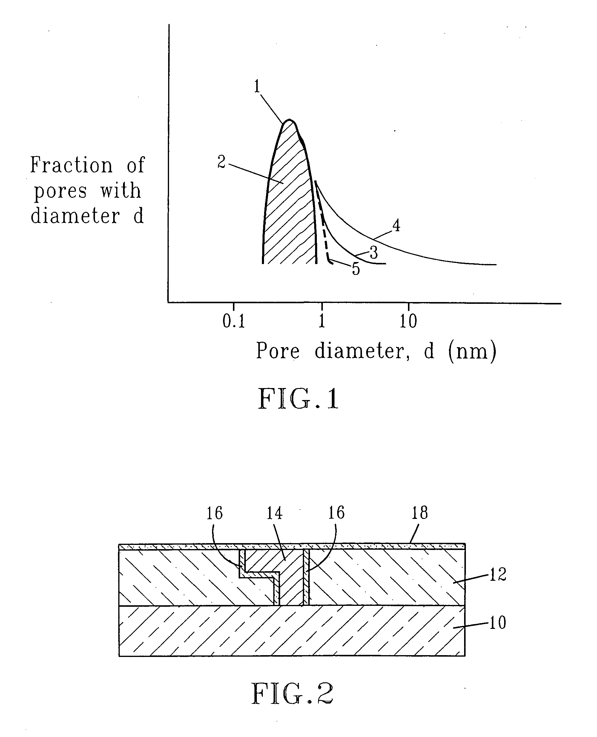
[0022] The second phase of the inventive porous dielectric material is a collection of pores having a pore size distribution (PSD) in which the PSD has a maximum that is less than about 1 nanometer, a full width at half maximum (FWHM) in the PSD of 1-3 nm, and with a fraction less than 0.1 of pores having a pore size of greater than about 1 nanometer. It is noted that the porous dielectric material of the present inv...
first embodiment
[0026] In addition to the first precursor, a second precursor (gas, liquid or vapor) is used. The second precursor in the present invention is a porogen such as a hydrocarbon with one double bond (i.e., an alkene molecule). The size of the alkene precursor is adjusted in order to adjust the typical dimension of the pores (the size of the maximum in the PSD). Referring to FIG. 1, curve 3 shows a schematic result obtained using 1-butene as the second precursor.
[0027] The second precursor employed in this embodiment of the present invention includes, but is not limited to: ethylene, propylene, butene, pentene, hexene, heptene, octene, and larger alkenes with greater than 8, preferably greater than 10, carbon atoms. The second precursor may also comprise a cyclic alkene containing at least one C═C double bond.
[0028] The present invention yet further provides for optionally adding an oxidizing agent such as O2, N2O, CO2 or a combination thereof to the gas mixture, thereby stabilizing th...
embodiment 2
[0042] In this embodiment, porous semiconducting materials are formed. The term “semiconducting” includes any element or compound having electrical conductivity intermediate between an insulator and a conductor. Examples of semiconducting materials that can be used in the present invention include, but are not limited to: Si, SiGe, SiGeC, SiC, Ge, GaAs, InAs, InP, AlN, GaN, InN, ternary alloys of Al, Ga, In, As, P, or N, silicon-on-insulators, SiGe-on-insulators, Ge-on-insulators, and other like materials.
[0043] The porous semiconductor materials of the present invention can be used as an element of a light emitting structure. Generally, light emitting structures require a crystalline semiconductor substrate. Also generally, the wavelength of the emitted light is adjusted by the band gaps of the semiconductor layers in the structure. These band gaps can be adjusted / modified either by doping of the crystalline semiconductor or changing the degree of crystallinity (feature size) and ...
PUM
 Abstract
Description
Claims
Application Information
 - R&D Engineer
- R&D Manager
- IP Professional
- Industry Leading Data Capabilities
- Powerful AI technology
- Patent DNA Extraction
Browse by: Latest US Patents, China's latest patents, Technical Efficacy Thesaurus, Application Domain, Technology Topic, Popular Technical Reports.
© 2024 PatSnap. All rights reserved.Legal|Privacy policy|Modern Slavery Act Transparency Statement|Sitemap|About US| Contact US: help@patsnap.com