Barrier Film For Flexible Copper Substrate And Sputtering Target For Forming Barrier Film
a barrier film and copper substrate technology, applied in the direction of vacuum evaporation coating, transportation and packaging, chemical coating, etc., can solve the problems of short circuit in the wiring on the circuit board, ineffectiveness, and barrier film peeling from the polyimide film, so as to prevent film peeling and achieve sufficient barrier
- Summary
- Abstract
- Description
- Claims
- Application Information
AI Technical Summary
Benefits of technology
Problems solved by technology
Method used
Image
Examples
example 1
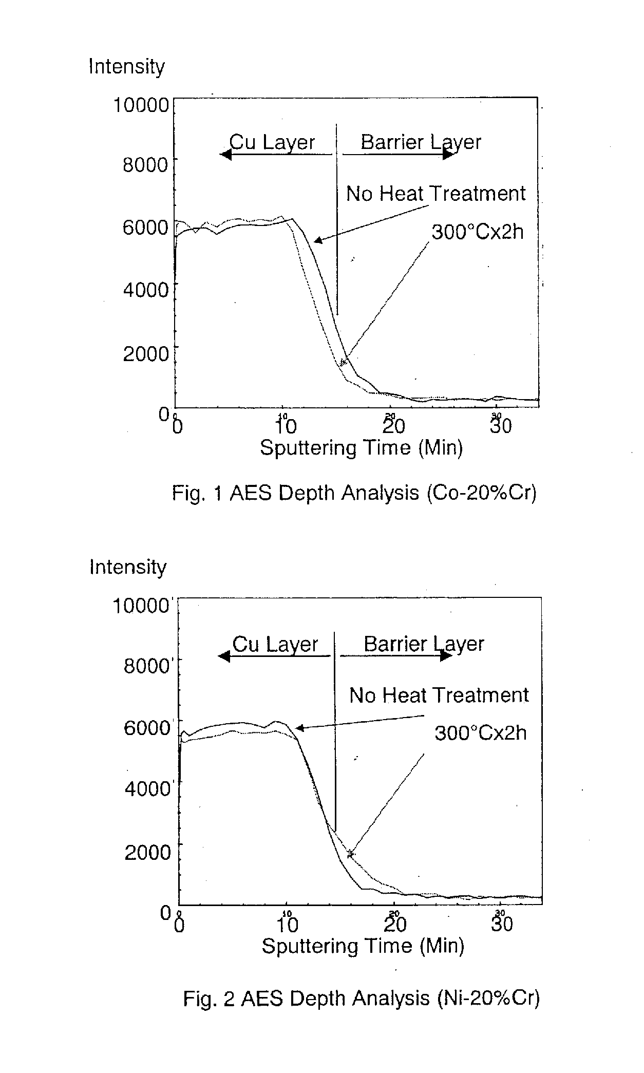
[0034] The composition of Co-20 wt % Cr was subject to melting and casting to prepare a Co—Cr ingot. This ingot was subject to hot forging and hot rolling at 1100° C., cooled, and thereafter subject to heat treatment at 500° C. for 2 hours and machined into a target. The grain size of this target was 280 μm. This target was further subject to finishing so that the average surface roughness Ra became 0.14 μm.
[0035] The Cr concentration of the target was 19.1 wt %, impurity components were 0.2 ppm of Na, 0.1 ppm of K, 0.02 ppm of U, 0.03 ppm of Th, the total content of metal components was 470 ppm, and the oxygen content was 10 ppm.
[0036] This target was bonded to the backing plate with indium, and the target side and the backing plate near the target were subject to bead blasting and coarsened until the Ra became 7.5 μm.
[0037] This target was used to prepare a barrier layer having a film thickness of 140 nm. As a result of analyzing the composition of the respective added componen...
example 2 to 8
[0048] A target was prepared with the same manufacturing method as Example 1, and such target having an alloy composition and relative magnetic permeability within the range of the present invention shown in Table 1 was used to form a barrier layer having a film thickness of 10 nm on a polyimide sheet having a thickness of 38 μm.
[0049] Further, the composition (wt %) of the respective added components of the barrier layer, the film thickness (nm) of the barrier layer, the film thickness uniformity (%) that measured the film thickness of the barrier layer at a 49-point, and the endurance test (hours) are similarly shown in Table 1. The film composition (wt %), film thickness (nm), and film thickness uniformity (%) of the barrier film of Examples 2 to 8 were all within the range of the present invention.
[0050] Further, a 20 nm Cu seed layer was deposited on this barrier layer with sputtering, and this was further subject to electroplating so as to form a Cu layer of 8 μm. An enduran...
PUM
| Property | Measurement | Unit |
|---|---|---|
| thickness | aaaaa | aaaaa |
| thickness | aaaaa | aaaaa |
| thickness | aaaaa | aaaaa |
Abstract
Description
Claims
Application Information
