Semiconductor device

a technology semiconductors, which is applied in the direction of semiconductor devices, basic electric elements, electrical equipment, etc., can solve the problems the modification of p-i-n junction diodes has a long reverse recovery time at shutoff, and the drawbacks of not meeting the requirements (1) and (5) have not been solved so far, so as to achieve the effect of improving properties

Inactive Publication Date: 2007-09-20
NGK INSULATORS LTD
View PDF21 Cites 12 Cited by
  • Summary
  • Abstract
  • Description
  • Claims
  • Application Information

AI Technical Summary

Benefits of technology

[0014]This achieves a heterojunction semiconductor device having a small leakage current and a high breakdown voltage during reverse blocking, and a high peak surge current value.
[0016]This achieves a P—N junction semiconductor device having a small leakage current and a high breakdown voltage during reverse blocking, a large output current at forward conduction, a short reverse recovery time at shutoff, and a high peak surge current value.
[0018]This achieves a semiconductor device having more improved properties producing the effects of the P—N junction semiconductor device as well as the effects resulting from the Schottky junction.

Problems solved by technology

Conventionally practical, silicon-employed P—N junction diode and its modified P-i-N junction diode have a drawback of long reverse recovery time at shutoff because of the occurrence of carrier injection from both P and N sides, that is, the above requirement (4) is not satisfied.
A SiC-employed Schottky barrier diode as disclosed in the above paper achieves the effect of increasing the breakdown voltage unlike a silicon-employed one, however, the drawbacks of not meeting the requirements (1) and (5) have not been solved so far.
SiC single crystal includes many crystal defects (specifically, tubular voids, what is called micropipes) and thus disadvantageously makes it difficult to manufacture with stability a device of relatively large area that can ensure sufficient output current, resulting in poor yields in manufacturing process.
Further, since a P—N junction diode employing SiC causes carrier recombination resulting from such crystal defects, the output current is more likely to be limited, so that the above requirement (3) is not satisfied.
A Schottky barrier diode employing group-III nitride semiconductor instead of silicon or SiC has also difficulty in solving the aforementioned drawbacks of not meeting the requirements (1) and (5).
Further, manufacturing a P—N junction diode having p- and n-type layers made of group-III nitride semiconductor instead of silicon or SiC is not practical because of technical difficulty in manufacturing P-type group-III nitride semiconductor having a high hole density with stability.

Method used


Image

  • Semiconductor device
  • Semiconductor device
  • Semiconductor device

Examples


first preferred embodiment

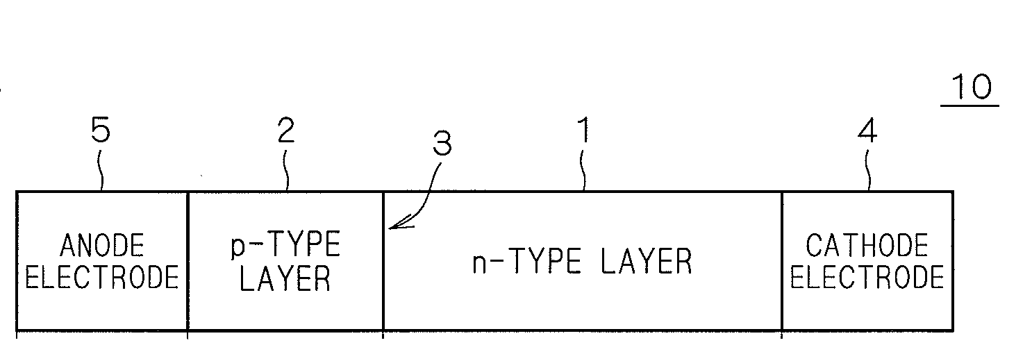
[0028]FIGS. 1A and 1B are diagrams for explaining the structure of a semiconductor device 10 according to a first preferred embodiment of the present invention. FIG. 1A schematically shows a sectional structure of the semiconductor device 10, and FIG. 1B shows the energy level of each layer constituting the semiconductor device 10. Each part in the respective drawings including FIGS. 1A and 1B is not always drawn at practical ratio. The structure of the semiconductor device 10 shown in FIG. 1A corresponds to the fundamental structure (conceptual structure) of various semiconductor devices by which the effects of the present invention can be achieved.

[0029]In the semiconductor device 10, an n-type layer 1 which is an n-type semiconductor layer and a p-type layer 2 which is a p-type semiconductor layer are joined at a junction 3, and a cathode electrode (cathode) 4 and an anode electrode (anode) 5 are provided next to the n-type layer 1 and p-type layer 2, respectively. In other words...

second preferred embodiment

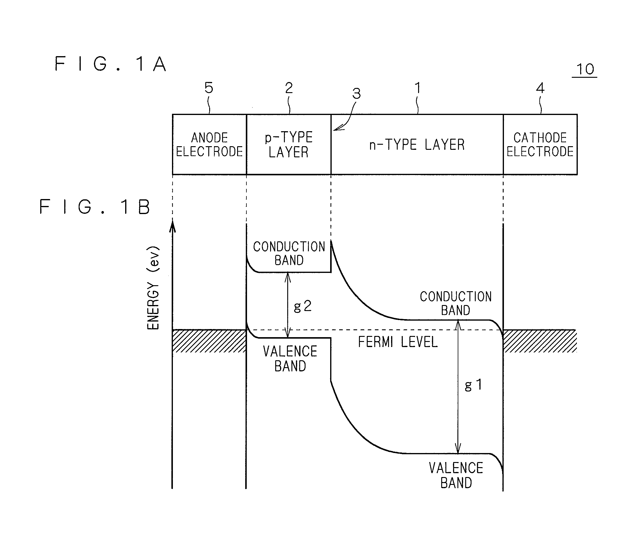
[0043]A more specific embodiment of a semiconductor device based on the conceptual structure described in the first preferred embodiment will now be described as a second preferred embodiment. FIG. 2 is a sectional view schematically showing the structure of a semiconductor device 20 according to the present embodiment. Among components of the semiconductor device 20 shown in FIG. 2, those achieving similar effects as those of the semiconductor device 10 are indicated by the same reference characters as in FIG. 1 and repeated explanation will be omitted.

[0044]The semiconductor device 20 shown in FIG. 2 features including a third electrode 6 not provided for the semiconductor device 10. The third electrode 6 is an electrode provided over the surfaces of the anode electrode 5 and n-type layer 1, and creates a Schottky junction with the n-type layer 1 at a junction 7 adjacent to the junction 3. In other words, the third electrode 6 covers the p-type layer 2 and anode electrode 5 deposi...

first example

[0049]In this example, a P—N junction vertical diode 110 which is one of specific embodiments of the semiconductor device 10 was prepared, and its properties were evaluated. FIG. 4A is a top view of the vertical diode 110, and FIG. 4B is a sectional view.

[0050]First, an n-type GaN substrate 1a having a thickness of 300 μm and an electron density of 1×10¹⁸ / cm3 was prepared. A GaN film 1b having an electron density of 1×10¹⁶ / cm3 was deposited thereon in a thickness of 5 μm by MOCVD to obtain the n-type layer 1.

[0051]Next, by ion implantation of Mg into part of the surface of the GaN film 1b and subsequent heat treatment for activating Mg, a field limiting ring 9 made of p-type GaN having a hole density of 1×10¹⁸ / cm3 was formed.

[0052]Subsequently, a Si layer doped with boron as an acceptor element of about 2×10²⁰ / cm3 so as to have a hole density of 1×10¹⁹ / cm3 or higher was formed as the p-type layer 2 on the n-type layer 1 (specifically, on the GaN film 1b) in the form of a disc having...


PUM


Abstract

A semiconductor device having small leakage current and high breakdown voltage during reverse blocking, small on-state resistance and large output current at forward conduction, short reverse recovery time at shutoff, and high peak surge current value is provided. An n-type layer is made of a group-III nitride, and a p-type layer is made of a group-IV semiconductor material having a smaller band gap than the group-III nitride. The energy level at the top of the valence band of the n-type layer is lower than the energy level at the top of the valence band of the p-type layer, so that a P—N junction semiconductor device satisfying the above requirements is obtained. Further, a combined structure of P—N junction and Schottky junction by additionally providing an anode electrode to be in Schottky contact with the n-type layer also achieves the effect of decreasing voltage at the rising edge of current resulting from the Schottky junction.

Description

FIELD OF THE INVENTION[0001]The present invention relates to a semiconductor device for power application, and more particularly to a power inverter or converter circuit device.DESCRIPTION OF THE BACKGROUND ART[0002]A semiconductor-employed switching device (transistor, thyristor, etc.) or rectifier device (diode) is widely used as a power inverter or converter circuit device. Under the present circumstances, a more compact device with lower losses is preferable for such semiconductor device for power application in order to meet future demands for higher power. While silicon has conventionally been used widely as a semiconductor material, wide band gap semiconductor materials having higher breakdown fields are being developed as next-generation semiconductor materials in light of the present circumstances. Since what is called wide band gap semiconductor materials such as SiC, group-III nitride semiconductor, etc. are expected to have low on-state resistance and high breakdown volt...

Claims


Application Information

Patent Timeline
Patent Type & Authority Applications(United States)
IPC IPC(8): H01L33/00H01L29/47H01L29/861H01L29/868H01L29/872
CPCH01L29/2003H01L29/267H01L29/872H01L29/861
Inventor MIYOSHI, MAKOTOKURAOKA, YOSHITAKA
Owner NGK INSULATORS LTD
Why Eureka
Try Eureka