Semiconductor device including internal voltage generation circuit

a technology of internal voltage generation and semiconductor devices, which is applied in the direction of electric pulse generator details, pulse techniques, instruments, etc., can solve the problems of high current consumption related to negative voltage, large variation in negative voltage, and high speed response at the negative voltage generation circuit. achieve the effect of low standby current and high speed operation

Active Publication Date: 2007-09-20
RENESAS ELECTRONICS CORP
View PDF3 Cites 22 Cited by
  • Summary
  • Abstract
  • Description
  • Claims
  • Application Information

AI Technical Summary

Benefits of technology

[0013]In view of the foregoing, a main object of the present invention is to provide a semiconductor device that allows high-speed operation with low standby current.
[0014]Another object of the present invention is to provide a semiconductor device that can prevent application of excessive stress in a burn-in test mode.
[0015]A further object of the present invention is to provide a semiconductor device having high operation speed.

Problems solved by technology

In this context, high-speed response at the negative voltage generation circuit is required since the substrate capacitance is not large as in a conventional DRAM and the current consumption related to negative voltage is increased.
Thus, there is a problem that variation in the negative voltage becomes great in a chip that has one negative voltage generation circuit incorporated for a plurality of memories.
However, the standby current cannot be increased in the field of battery-driven portable equipment in which this type of DRAM is incorporated, since there is a demand for lower power consumption by reduction in operating voltage and consumed current.
This type of DRAM also poses the problem of increase in circuit failure caused by excessive stress applied to the transistor during a burn-in test mode.
Further, this type of DRAM poses the problem that the operation speed is reduced due to the reduction in power supply voltage and / or increase in ground voltage in a circuit operation mode.
In addition, this type of DRAM is easily affected by noise.
Moreover, there was a problem that a semiconductor integrated circuit device including a plurality of such DRAMs exhibited unstable circuit operation due to the reduction in power supply voltage and / or increase in ground voltage.

Method used


Image

  • Semiconductor device including internal voltage generation circuit
  • Semiconductor device including internal voltage generation circuit
  • Semiconductor device including internal voltage generation circuit

Examples


first embodiment

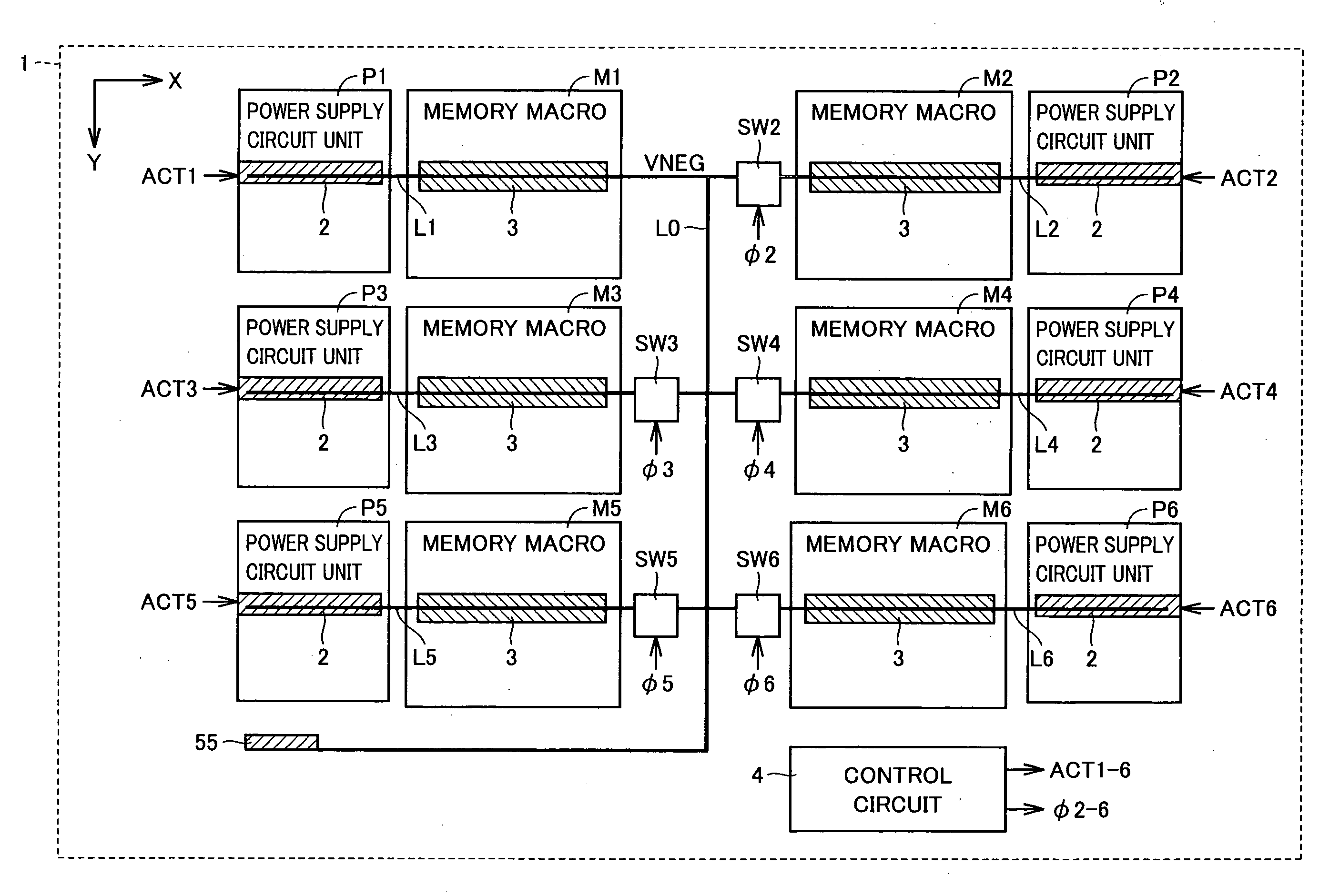
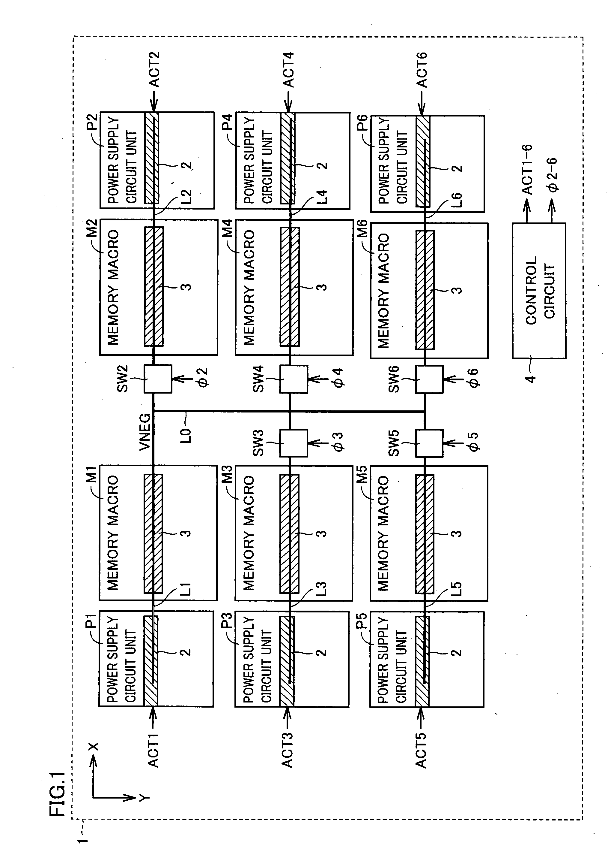
[0057]Referring to FIG. 1, a semiconductor integrated circuit device according to a first embodiment of the present invention includes a semiconductor substrate 1, a plurality (six in the drawing) of memory macros M1-M6 formed at the surface of semiconductor substrate 1, each for a data write / read operation independently, six power supply circuit units P1-P6 provided corresponding to memory macros M1-M6, respectively, negative voltage supply lines L0-L6 and switch circuits SW2-SW6 for supplying a negative voltage VNEG generated at a negative voltage generation circuit 2 in each of power supply circuit units P1-P6 to a word line driver 3 in memory macros M1-M6, and a control circuit 4 generating control signals ACT1-ACT6 and φ2-φ6.

[0058]Negative voltage supply line L0 is arranged at the middle of semiconductor substrate 1, extending in the Y direction (vertical direction) in the drawing. Memory macros M1, M3 and M5 are arranged in the Y direction at the left side of negative voltage ...

second embodiment

[0094]A semiconductor integrated circuit device including a DRAM using a P channel MOS transistor as the transfer gate of a memory cell is subjected to a burn-in test (acceleration test), likewise a conventional DRAM, for screening early failure. In a burn-in test, a voltage higher than that of a general level is applied. The application of negative voltage VNEG to this type of semiconductor integrated circuit device in a burn-in test may apply excessive stress across the source and drain of the transistor, leading to the possibility of increasing early failure.

[0095]In view of this possibility, there is an approach to dispose an internal voltage switch circuit 56 to switch negative voltage VNEG to ground voltage GND in order to prevent application of excessive stress during a burn-in test, at each of power supply circuit units P1-P6, as shown in FIG. 11. Specifically, this semiconductor integrated circuit device has negative voltage supply lines L1-L6 provided corresponding to memo...

third embodiment

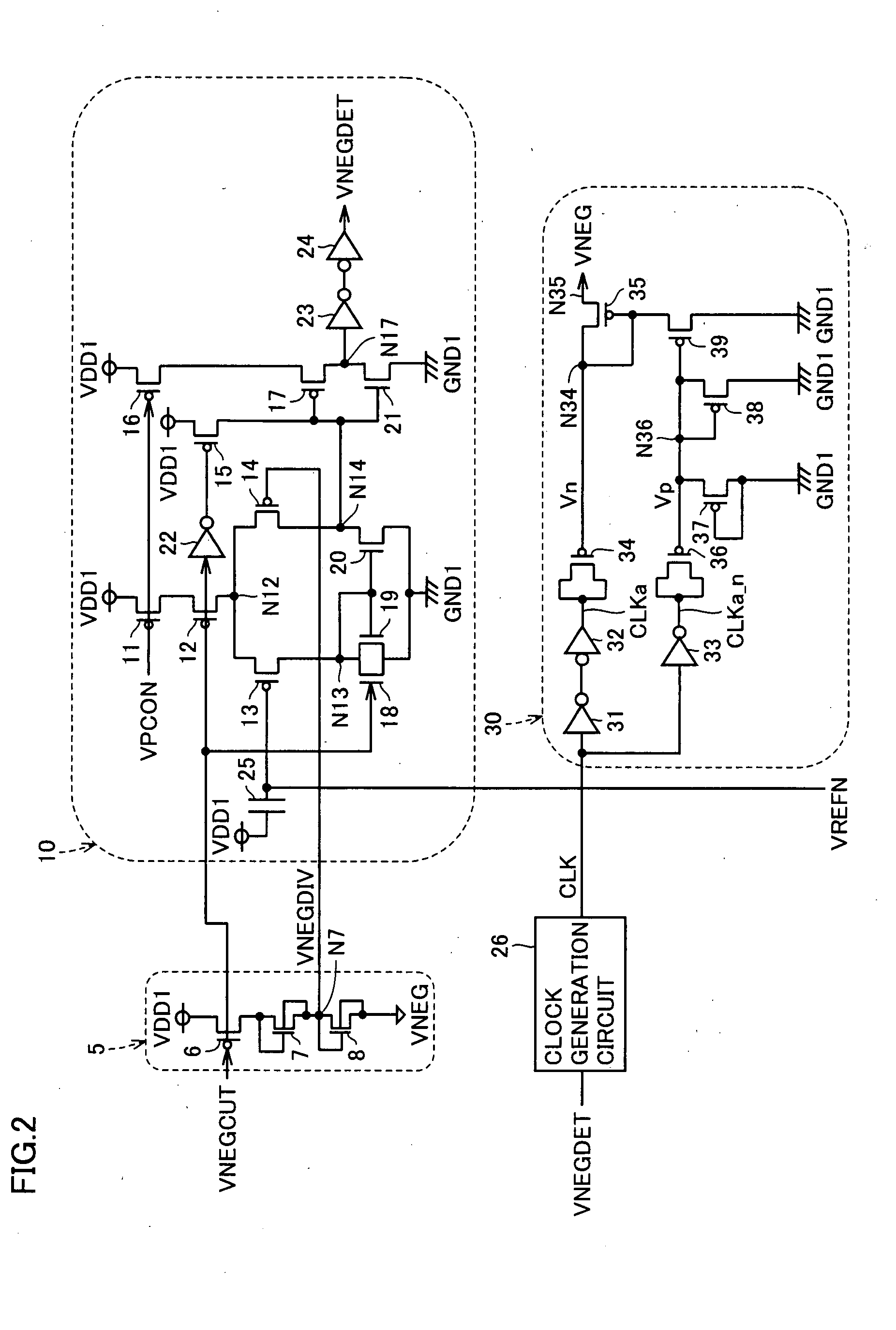
[0098]Reference voltage VREFN is supplied from one reference voltage generation circuit formed of intermediate voltage generation circuit 40 and buffer circuit 41 to negative voltage generation circuit 2 of six power supply circuit units P1-P6, as shown in FIG. 3. If the reference voltage generation circuit is disposed at power supply circuit unit P1, for example, the routing length of reference voltage line L10 that supplies reference voltage VREFN from the reference voltage generation circuit to negative voltage generation circuit 2 of power supply circuit unit P6 is increased significantly, leading to the possibility of noise generation at reference voltage line L1. In view of this possibility, this type of semiconductor integrated circuit is provided with shield lines 60 and 61 sandwiching reference voltage line L10 to protect reference voltage line L10 from noise as shown in FIG. 13. Shield lines 60 and 61 are connected to the line of ground voltage GND 7 dedicated to shielding...


PUM


Abstract

A semiconductor integrated circuit device has a negative voltage generation circuit provided at each power supply circuit unit for six memory macros. Therefore, the response with respect to variation in a negative voltage is increased. In a standby mode, a negative voltage supply line for the six memory macros is connected by a switch circuit, and only a negative voltage generation circuit of one power supply circuit unit among six negative voltage generation circuits of the six power supply circuit units is rendered active. Thus, increase in standby current can be prevented.

Description

BACKGROUND OF THE INVENTION[0001]1. Field of the Invention[0002]The present invention relates to semiconductor devices, particularly a semiconductor device including an internal voltage generation circuit.[0003]2. Description of the Background Art[0004]In a general DRAM (Dynamic Random Access Memory), an N channel MOS transistor is used as a transfer gate of a memory cell. A positive voltage is employed as the voltage for selection, applied to a word line, when a memory cell is rendered active. A negative voltage generation circuit generating a negative voltage lower than the ground voltage is incorporated in this DRAM. The negative voltage is used as a substrate bias voltage to control the substrate effect of a transistor.[0005]In this context, variation in the level of the negative voltage is suppressed due to the large capacitance of the substrate. Further, high-speed response at the negative voltage generation circuit formed of a negative voltage detection circuit and a negative...

Claims


Application Information

Patent Timeline
Patent Type & Authority Applications(United States)
IPC IPC(8): G11C5/14H03K17/16
CPCG11C5/025G05F1/468G11C5/147G11C11/4074G11C5/14
Inventor AKIYAMA, MIHOKOIGAUE, FUTOSHIYOSHINAGA, KENJIMATSUMURA, MASASHIMORISHITA, FUKASHI
Owner RENESAS ELECTRONICS CORP
Why Eureka
Try Eureka