

Compound Semiconductor Light-Emitting Device
a technology of compound semiconductors and light-emitting devices, which is applied in the direction of semiconductor devices, basic electric elements, electrical equipment, etc., can solve the problems of low resistance, low resistance, and failure of pn-junction compound semiconductor light-emitting devices including p-type boron-phosphide-based semiconductor layers to achieve low forward voltage, and achieve high surface flatness
- Summary
- Abstract
- Description
- Claims
- Application Information
AI Technical Summary
Benefits of technology
Problems solved by technology
Method used
Image

Examples
example 1
[0038] The present invention will next be described in detail taking, as an example, fabrication of a pn-junction compound semiconductor LED having a p-type boron-phosphide-based semiconductor layer joined to an undoped Group III nitride semiconductor layer.
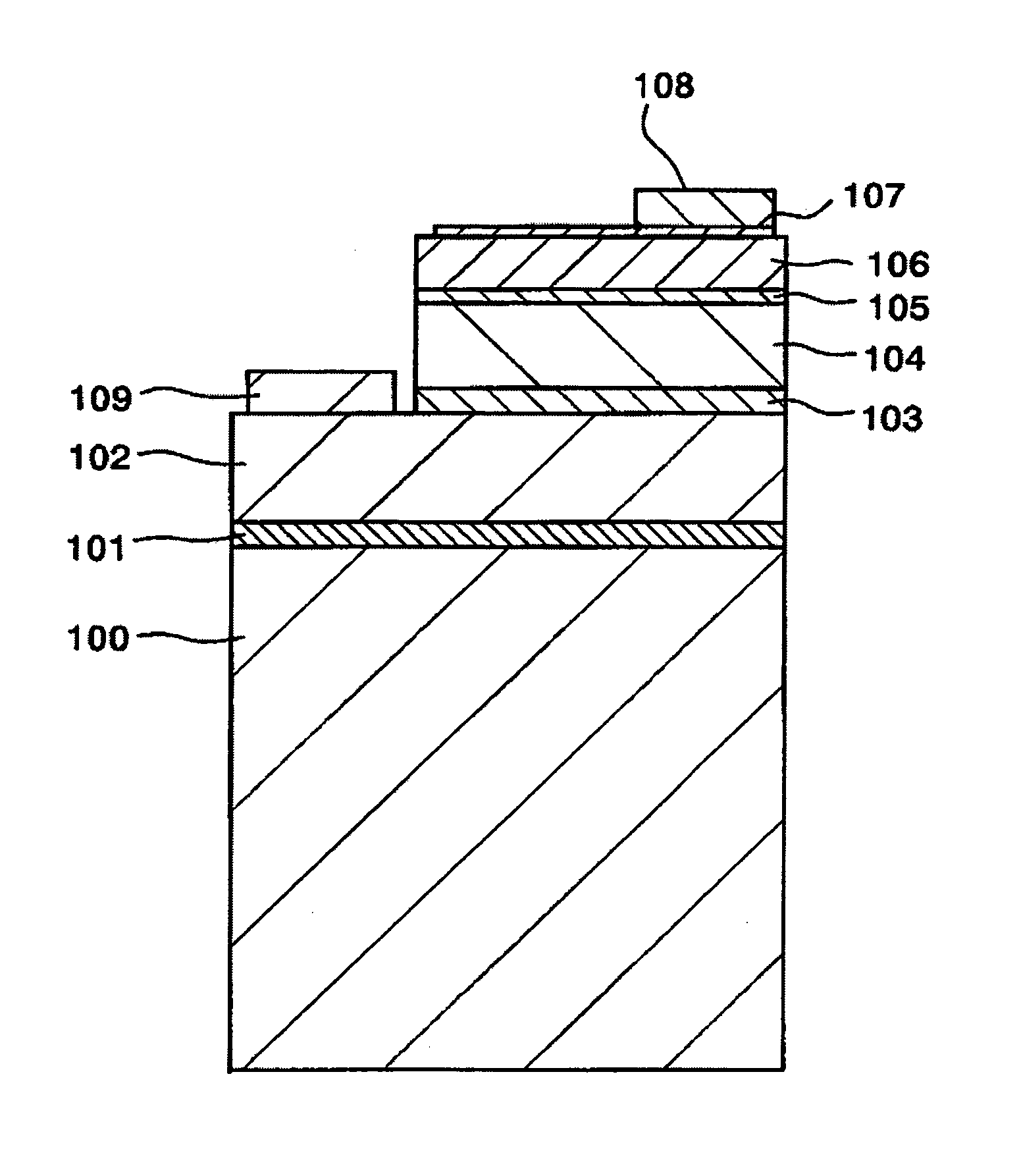
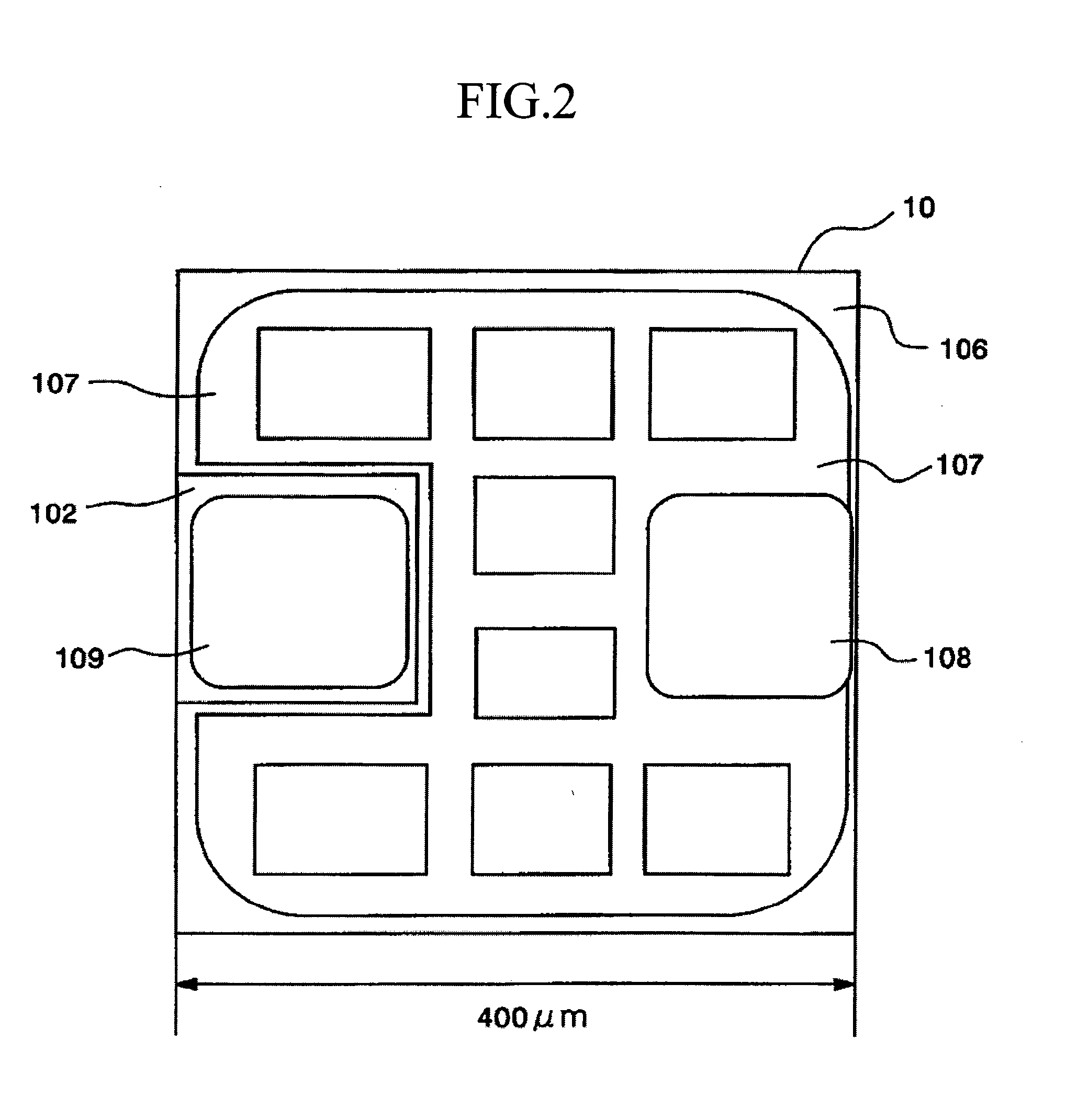
[0039]FIG. 1 schematically shows a cross-section of an LED 10 having a double-hetero (DH) junction structure. FIG. 2 is a schematic plan view of the LED 10.
[0040] The LED 10 was fabricated from a stacked structure formed of the following layers (1) to (6) sequentially grown on a (0001)-sapphire (α-Al2O3 single crystal) substrate 100. [0041] (1) a buffer layer 101 (thickness (t): 15 nm) composed of undoped GaN [0042] (2) a lower cladding layer 102 composed of a silicon (Si)-doped n-type GaN layer (carrier concentration (n)=7×1018 cm−3, t=3 μm) [0043] (3) a light-emitting layer 103 having a well layer composed of an undoped n-type Ga0.86In0.4N layer [0044] (4) an upper cladding layer 104 composed of a magnesium (Mg)-doped p-type ...
example 2
[0055] The present invention will next be described in detail taking, as an example, fabrication of a pn-junction compound semiconductor LED having a p-type boron aluminum phosphide layer joined to an undoped Group III nitride semiconductor layer.
[0056] On the sapphire substrate described in Example 1, the same constituent layers as employed in Example 1; i.e., a buffer layer, an n-type lower cladding layer, a light-emitting layer, a p-type upper cladding layer, and an undoped Al0.10Ga0.90N layer were formed. Subsequently, an undoped p-type boron aluminum phosphide (compositional formula: B0.98Al0.02P) layer was provided so as to be joined to the Group III nitride semiconductor layer composed of the undoped Al0.10Ga0.90N layer. The B0.98Al0.02P layer serving as the p-type boron-phosphide-based semiconductor layer was formed so as to have a carrier concentration of about 7×1017 cm−3 and a thickness of 200 nm.
[0057] Through analysis of electron diffraction patterns, all of the n-typ...
PUM
 Abstract
Description
Claims
Application Information