Driver circuit for switching device

a technology of driving circuit and switching device, which is applied in the direction of electronic switching, pulse generator, pulse technique, etc., can solve the problems of large temperature dependence of on-resistance, and achieve the effect of small mounting area of power semiconductor device and small size of semiconductor apparatus

Inactive Publication Date: 2007-09-27
HITACHI LTD
View PDF14 Cites 43 Cited by
  • Summary
  • Abstract
  • Description
  • Claims
  • Application Information

AI Technical Summary

Benefits of technology

[0008]According to the gate driver circuit for power semiconductor device, it is possible to make the wide gap semiconductor device made of SiC or the like operate up to high temperatures, make the mounting area of the power semiconductor device small, and make the size of the semiconductor apparatus small.

Problems solved by technology

However, it is known that the dependence of the on-resistance upon the temperature is large in unipolar devices. FIG. 2 shows relations between the junction temperature and the mounting area under different cases of the dependence upon the temperature.

Method used


Image

  • Driver circuit for switching device
  • Driver circuit for switching device
  • Driver circuit for switching device

Examples


first embodiment

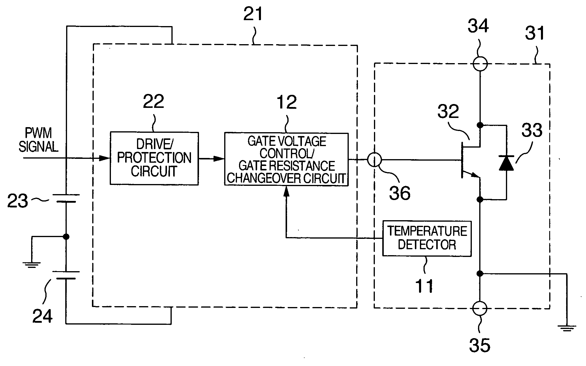
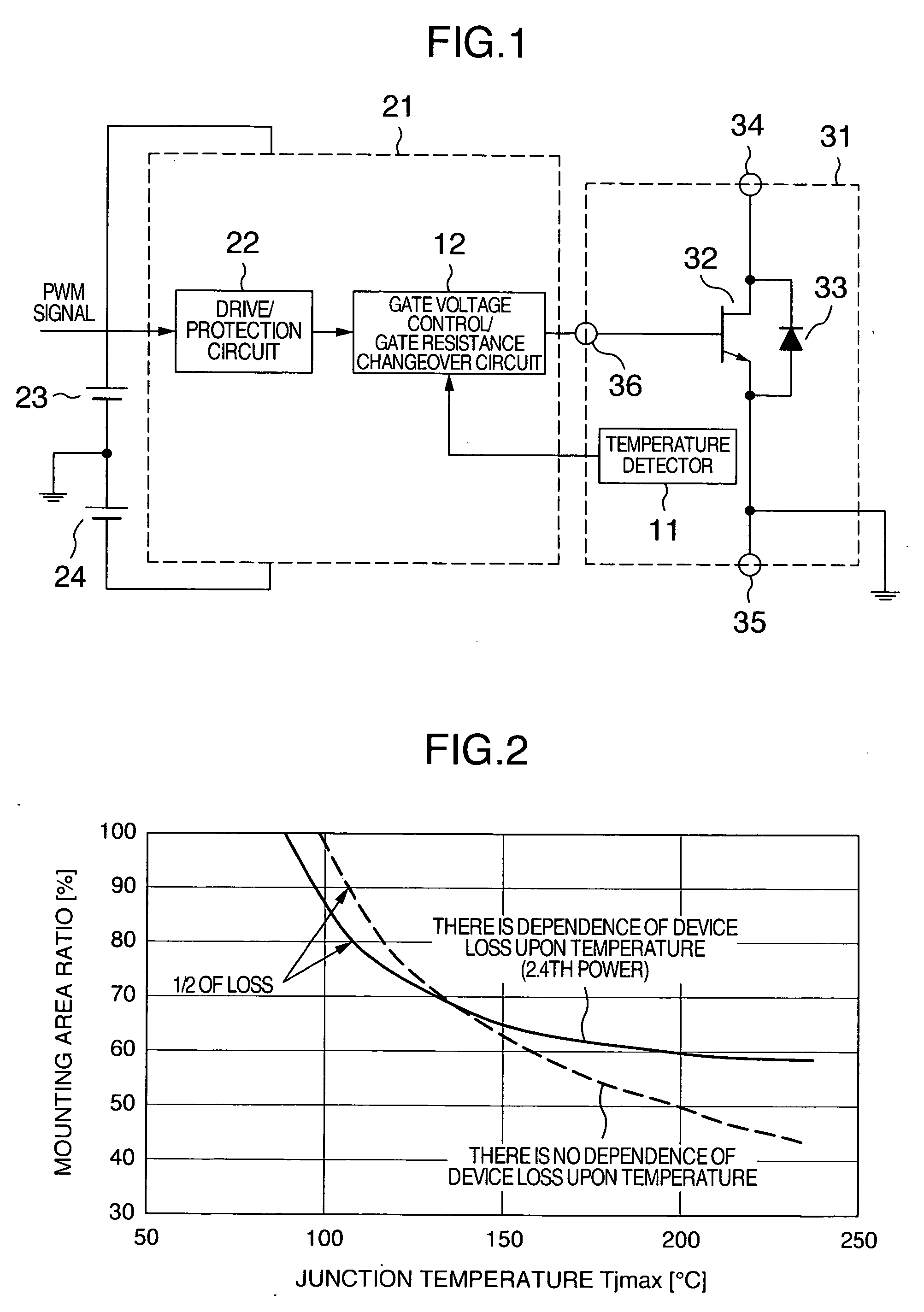
[0024]FIG. 1 shows a block diagram of a driver circuit for power semiconductor device according to a first embodiment. The reference numeral 23 indicates a positive bias power source for a driver circuit 21 and the reference numeral 24 indicates a negative bias power source for the driver circuit 21. A power module 31 shown in FIG. 1 is connected to the driver circuit 21. In the power module 31, a freewheeling diode 33 is connected in parallel with a SiC junction-type FET (SiC-JFET) 32 which is a wide gap semiconductor switching device.

[0025]In the present embodiment, a temperature detector 11 in the power module and a gate voltage control / gate resistance changeover circuit 12 are provided. A drive / protection circuit 22 is also provided. The temperature of the power semiconductor switching device is detected. If the detected temperature is higher than a predetermined temperature, the gate drive voltage is raised or the gate drive resistance is reduced.

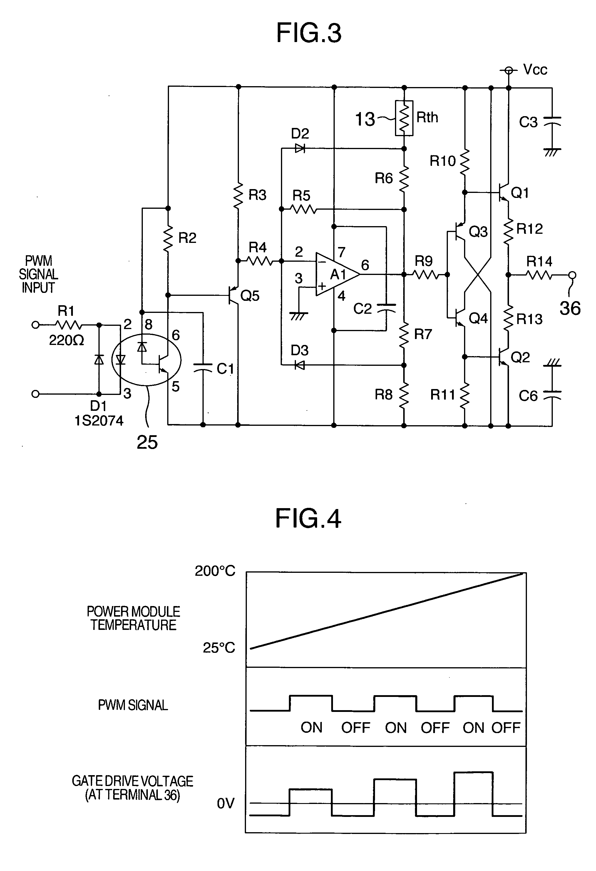
[0026]FIG. 3 is a circuit diagr...

second embodiment

[0027]FIG. 5 shows a block diagram of a driver circuit for power semiconductor device according to a second embodiment. The second embodiment differs from the first embodiment in a wide gap semiconductor switch device. In the present embodiment, a SiC-MOSFET 37 is used as shown in FIG. 5. If the SiC-MOSFET 37 is used, a body diode is incorporated and consequently there is no problem without the freewheeling diode 33.

[0028]This embodiment provides a device having large dependence of the on-resistance upon the temperature with very effective control unit. Among wide gap semiconductors made of SiC or the like, the unit is effective especially to driver circuits for junction-type FETs (SiC-JFETs) and MOSFETs. In bipolar transistors and IGBTs of wide gap semiconductor made of SiC or the like as well, however, the switching loss increases as the temperature rises. Accordingly, the total loss (conduction loss+turn-on loss+turn-off loss) at the time of high temperatures is reduced by applyi...

third embodiment

[0030]FIG. 6 shows a block diagram of a driver circuit for power semiconductor device according to a third embodiment. The same components as those in the first embodiment are denoted by like reference numerals. The present embodiment has a configuration for detecting the temperature of the power module and varying the gate resistance.

[0031]FIG. 7 shows a circuit diagram of the driver circuit for power semiconductor device according to the present embodiment. The same components as those in the first embodiment are denoted by like reference numerals. In the present embodiment, temperature deciders 14 are provided as shown in FIG. 7. If the temperature of the device in the power module is high, then MOSFETs shown in FIG. 7 are turned on to reduce the gate resistance. At the time of drive at high temperatures, therefore, the gate resistance is reduced and consequently it is possible to raise the speed of di / dt and dv / dt and reduce the loss in the power device. At the time of turn off ...


PUM


Abstract

A driver circuit that lowers the dependence of the loss in the wide gap semiconductor device upon the temperature is provided. A gate driver circuit for voltage driven power semiconductor switching device includes a power semiconductor switching device, a driver circuit for supplying a drive signal to a gate terminal of the switching device with reference to an emitter control terminal or a source control terminal of the switching device, and a unit for detecting a temperature of the switching device. The temperature of the power semiconductor switching device is detected, and a gate drive voltage or a gate drive resistance value is changed based on the detected temperature.

Description

BACKGROUND OF THE INVENTION[0001]The present invention relates to a driver circuit for wide gap semiconductor switching device made of SiC, GaN or the like.[0002]As for the wide gap semiconductor switching devices, silicon carbide (SiC), gallium nitride (GaN) or the like is drawing the attention. These materials have a dielectric breakdown voltage strength that is approximately ten times as high as that of Si, and a drift layer for ensuring the withstand voltage can be made thin to approximately one tenth. Therefore, it is possible to implement a lower on-voltage of power devices. Even in a high withstand voltage region in which only bipolar devices can be used with Si, therefore, it becomes possible to use unipolar devices in wide gap semiconductor devices made of SiC or the like. In Si-IGBTs which form the main stream of power devices at the present time, there is a built-in voltage of approximately 1 V. In MOSFETs and junction-type FETs (abbreviated to JFETs) which are unipolar d...

Claims


Application Information

Patent Timeline
Patent Type & Authority Applications(United States)
IPC IPC(8): H01L23/62
CPCH01L27/0248H01L2924/0002H01L2924/00H02M1/08H02M1/327
Inventor ISHIKAWA, KATSUMIFUNAKOSHI, SUNAOSAKAMOTO, KOZOONOSE, HIDEKATSU
Owner HITACHI LTD
Why Eureka
Try Eureka