

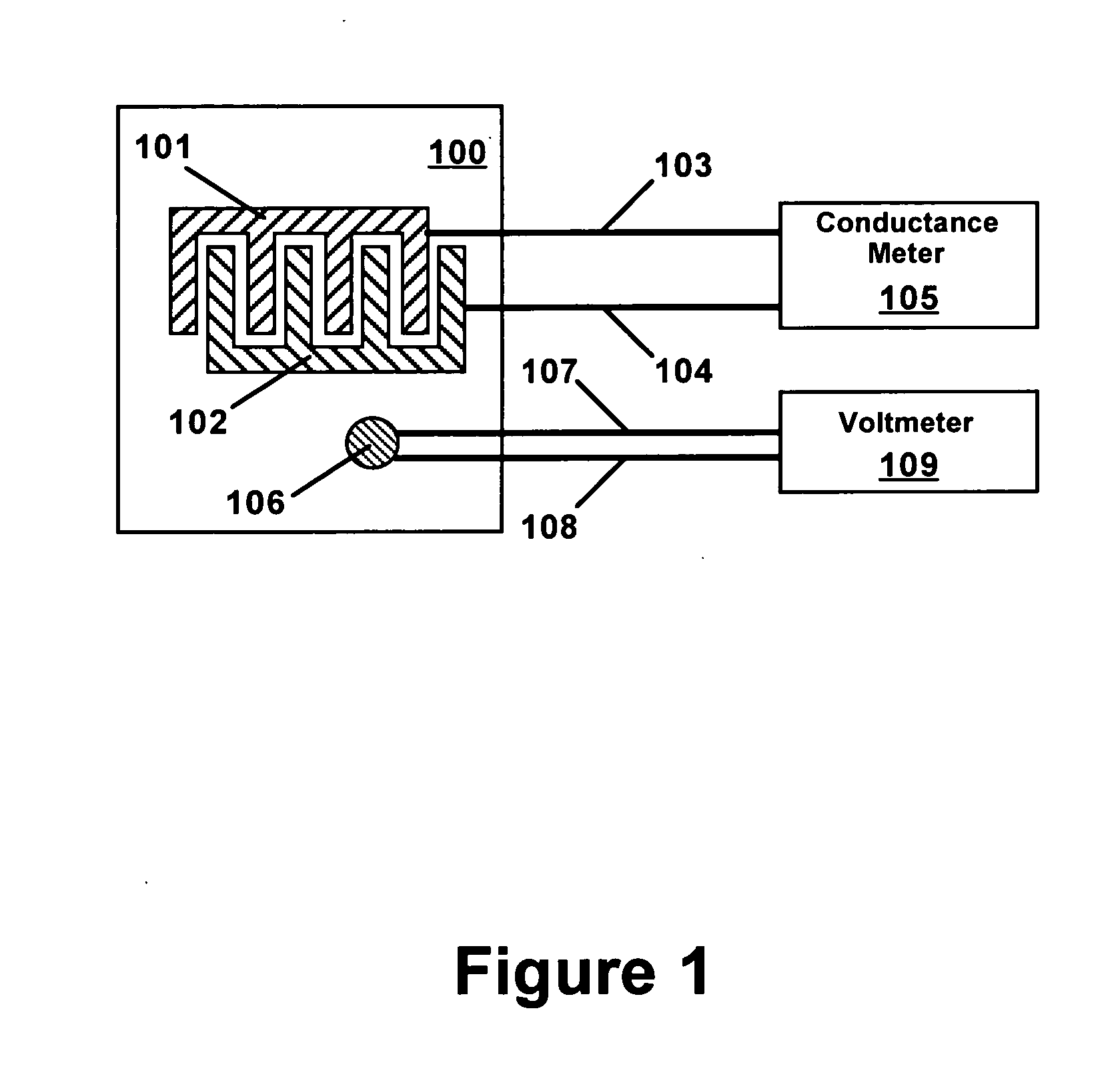
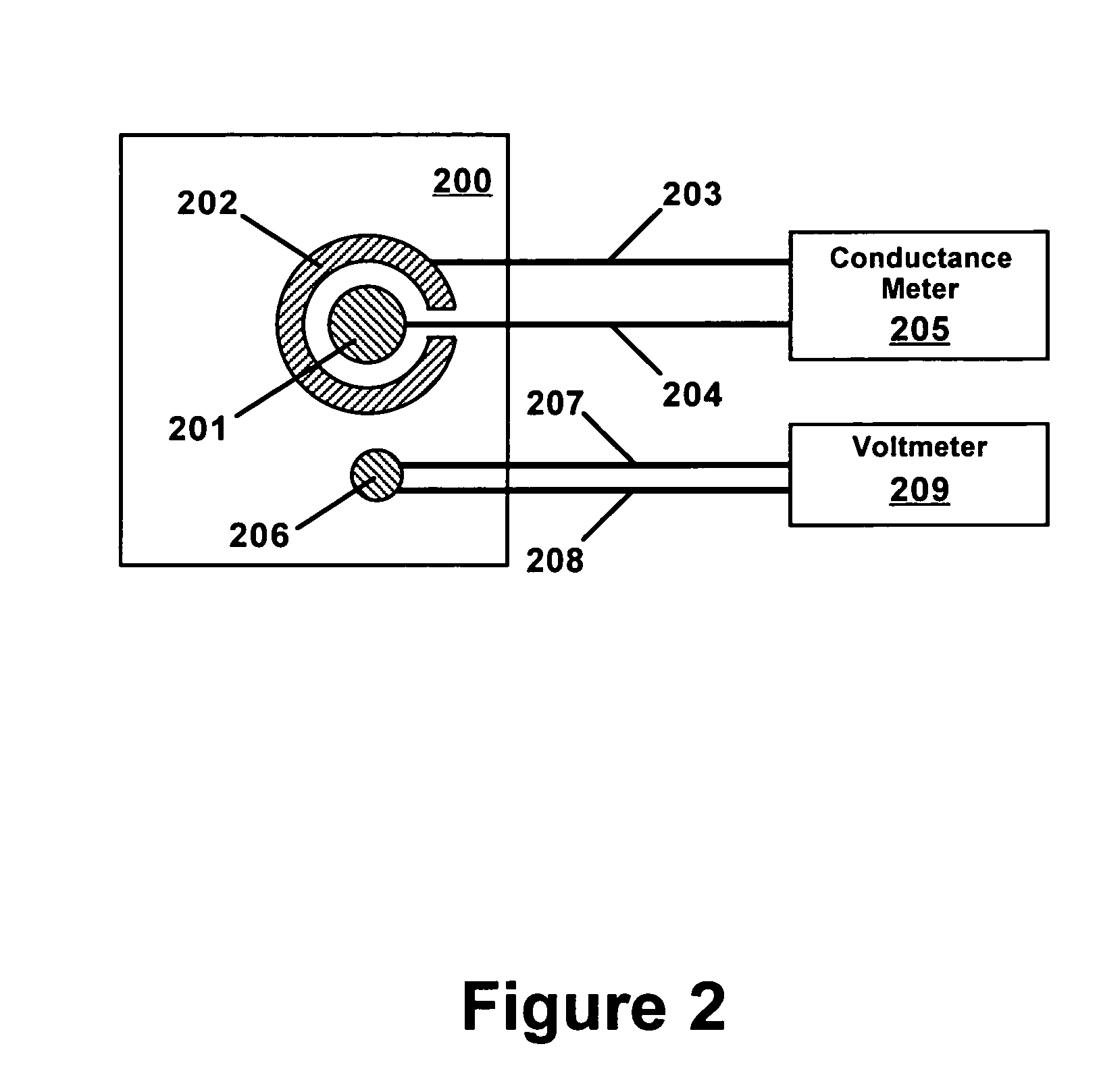
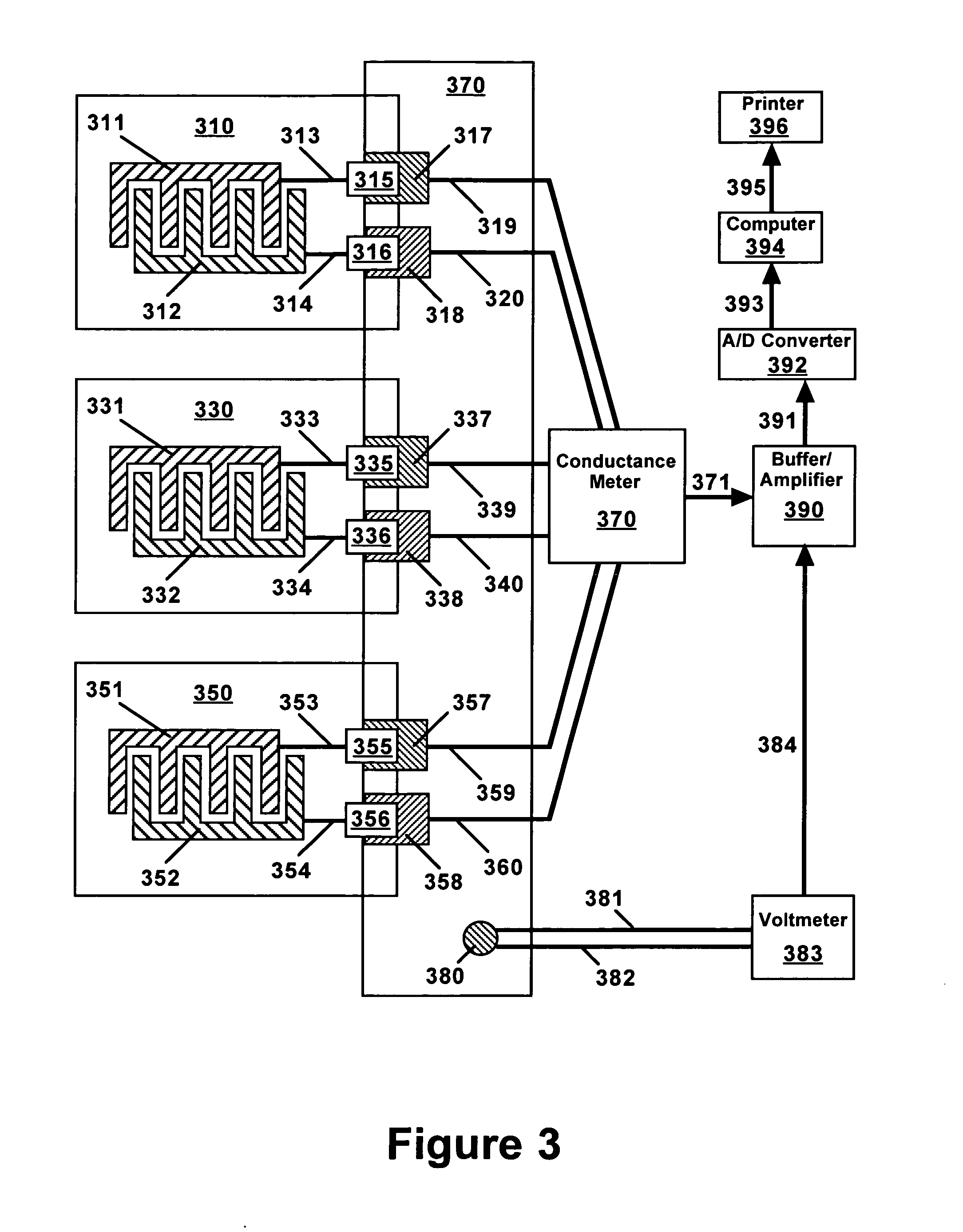
Thermoconductimetric analyzer for soldering process improvement
a technology of thermal conductivity and analyzer, which is applied in the direction of fluid resistance measurement, instruments, nuclear elements, etc., can solve the problems of weak solder joints having low electrical resistance, failure of circuits, and the need for sufficient stiffness of the solder paste, so as to minimize the defects of wave soldering, improve the soldering performance, and minimize the defect during reflow soldering
- Summary
- Abstract
- Description
- Claims
- Application Information
AI Technical Summary
Benefits of technology
Problems solved by technology
Method used
Image

Examples
example 1
[0071]FIG. 6 shows illustrative conductance-temperature time profiles measured for reflow of two commercial solder flux formulations (Kester 244 and Kester 256GS) using the low temperature profile. A measurable conductance is evident for both of the solder fluxes at room temperature, indicating some flux activity that might limit the shelf life of the flux. The higher room-temperature conductance evident for the Kester 256GS indicates that this flux would tend to lose activity more rapidly during storage and would have a shorter shelf life. Actual shelf life tests indicated a shelf life of 4 months for the Kester 256GS flux, and 6 months for the Kester 244 flux.
[0072] Beginning at about 45° C. (0.5 minutes) in FIG. 6, the conductance of the Kester 256GS flux increased sharply, indicating increasing flux activity as the flux activator dissolved and dissociated in the flux solvent. The activity of the Kester 244 flux, as indicated by the measured conductance, is seen to lag that of t...
example 2
[0076]FIG. 7 shows illustrative conductance-temperature time profiles measured for the two commercial solder flux formulations of Example 1 (Kester 244 and Kester 256GS) using the medium temperature profile rather than the low temperature profile. Such an increase in temperature may be required, for example, for reflow soldering with tin-silver-copper solder, which has a higher melting point than the conventional tin-lead solders. For the medium temperature profile, the Kester 256GS flux exhibited the same two conductance peaks but the performance was improved, as indicated by significantly higher flux activity at the maximum soldering temperature. On the other hand, the activity of the Kester 244 flux, although tending to be high, exhibited considerable variation at the higher temperatures, indicating that some components of the Kester 244 activator system may be too volatile at the higher temperatures of the medium temperature profile. In this case, the Kester 256GS flux may be pr...
example 3
[0077]FIG. 8 shows illustrative conductance-temperature time profiles measured for the two commercial solder flux formulations of Examples 1 and 2 (Kester 244 and Kester 256GS) using the high temperature profile rather than the low temperature profile. For the high temperature profile, the Kester 256GS flux also exhibited the same two conductance peaks and the performance was further improved, as indicated by significantly higher flux activity at the maximum soldering temperature (compared to the medium temperature profile). By contrast, the activity of the Kester 244 flux was decreased at the higher temperatures of the high temperature profile (compared to the medium temperature profile).
[0078] From the results given in Examples 1-3, it is apparent that the Kester 256GS flux is preferred for the high temperature profile, whereas the Kester 244 flux would give better results for soldering parts with relatively poor solderability with the low temperature profile. Based on its lower ...
PUM
| Property | Measurement | Unit |
|---|---|---|
| voltages | aaaaa | aaaaa |
| thick | aaaaa | aaaaa |
| thick | aaaaa | aaaaa |
Abstract
Description
Claims
Application Information