Electrode Substrate and Its Manufacturing Method

a technology of electrochemical substrates and manufacturing methods, which is applied in sustainable manufacturing/processing, identification means, instruments, etc., can solve the problems of easy advancement of contamination of substrates, and easy generation of defective surface layers, so as to reduce the driving voltage of organic el elements, improve the electrical stability of elements, and reduce the effect of production costs

Inactive Publication Date: 2007-10-25
IDEMITSU KOSAN CO LTD
View PDF22 Cites 19 Cited by
  • Summary
  • Abstract
  • Description
  • Claims
  • Application Information

AI Technical Summary

Benefits of technology

[0089] As described above, according to the electrode substrate of the invention, the electric stability thereof is improved since an electrode in which a defective surface layer is decreased is used. Accordingly, when this electrode substrate is used as, for example, an anode of an organic EL element, an advantageous effect that the lifespan of the element can be made long can be produced. Furthermore, an advantageous effect that a rise in the driving voltage of this organic EL element can be restrained is produced. Additionally, the heat resistance of this organic EL element can be improved.
[0090] According to the invention, an electrode substrate fitted to, for example, the production of a display device of

Problems solved by technology

However, when three organic substances (herein after referred to merely as the organic substances) are used, the production process becomes complicated.
[1] In the case of producing a CCM substrate, the number of steps for producing the substrate is large so that contamination of the substrate advances easily and a defective surface layer is easily generated on the surface of its anode.
In particular, the surface of a transparent electrode of IZO or the like is easily damaged by an excessive washing step or residues resu

Method used


Image

  • Electrode Substrate and Its Manufacturing Method
  • Electrode Substrate and Its Manufacturing Method
  • Electrode Substrate and Its Manufacturing Method

Examples


example 1

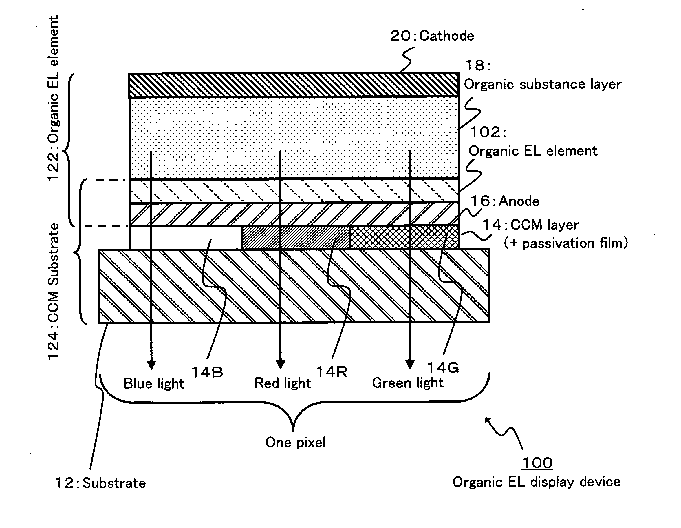
[0245] In Example 1, it is demonstrated that in the case of forming the surface protecting layer 102 on the anode 16 on the CCM substrate 124, which may be called the CCM electrode substrate, whereby the CCM substrate 124 is used to produce the organic EL display device 122, which may be called the CCM panel, performances of the organic EL display device 122 become high.

[0246] [1] Production 1 of the CCM Substrate 124 (Color Converting Substrate) (Up to the Formation of a Color Converting Film)

[0247] AV259 BK (manufactured by Nippon Steel Chemical Co., Ltd.) was applied as a material of a black matrix (BM) onto a 102 mm×133 mm×1.1 mm supporting substrate (OA2 glass, manufactured by Nippon Electric Glass Co., Ltd.) by spin coating, and then the resultant was exposed to ultraviolet rays so as to give a lattice form pattern. The resultant was developed with a 2% solution of sodium carbonate in water, and then baked at 200° C. to form a black matrix pattern (film thickness: 1.5 μm).

[...

embodiment 2

Example Having a Structure which Contains TFTs

[0291] In the example illustrated in FIG. 1, the anode 16 is illustrated on the CCM layer 14. In FIG. 1, the system for driving this anode 16 is not particularly described. It is preferred to drive the anode 16 by means of, for example, TFTs (thin film transistors). Such a structure is illustrated in FIG. 3. In FIG. 3, a schematic sectional view of a moiety for one color in the one pixel illustrated in FIG. 1 is shown. In other words, a moiety for any one color of the red, blue and green colors in FIG. 1 is shown.

[0292] As illustrated in this figure, in the present embodiment, a CCM layer 14 is formed in a substrate 12. On the CCM layer 14, an overcoat layer 210 and a passivation film 212 are formed. On the passivation film 212, a gate 226 of a thin film transistor 220 is formed, and further an insulating film 230 is laminated thereon so as to cover the gate.

[0293] An anode 16, and a drain 224 and a source 222 of the thin film transis...


PUM


Abstract

The purpose is to remove surface-defective layer existing on the surface of an anode on a CCM substrate, protect the anode surface, prevent a drive voltage of an organic EL element from rising, and maintain uniformity of luminescence. On a substrate (12) a CCM layer (14) for converting light wavelength is formed. On the CCM layer (14) an anode (16) of IZO is formed. On the anode (16) a surface protective layer (18) containing an inorganic compound is formed by an inductively coupled RF plasma support magnetron sputtering. A preferable inorganic compound is SiO2. The surface defective layer of the anode (16) can be removed by the sputtering and the state of being removed can be held by the inorganic compound. Therefore the electrical stability of the anode (16) can be maintained for a long time, thereby improving the display quality of an organic EL display (100).

Description

TECHNICAL FIELD [0001] The present invention relates to a structure of a substrate of an organic EL element, and a method for producing the same. In particular, the invention relates to an electrode substrate used in an organic EL element using the CCM method. More specifically, the invention relates to a color changing (CCM) substrate in which a measure is taken against a deterioration in the surface of a transparent electrode which is an anode of the substrate. BACKGROUND ART A. Technical Background [0002] In recent years, attention has been paid to organic EL (electroluminescence) elements from the viewpoint of application thereof to light emitting devices or display devices. For example, there has been advanced the use thereof as color and full-color display devices in information display instruments, on-vehicle display devices, or the like. [0003] (1) Basic Structure of an Organic EL Element [0004] In general, an organic EL element has a structure in which a transparent electro...

Claims


Application Information

Patent Timeline
IPC IPC(8): H01J1/62H01J9/02G09F9/30H01B5/14H01L27/32H01L51/00H01L51/52H05B33/02H05B33/12H05B33/14H05B33/28
CPCH01L27/322H01L27/3248Y02E10/549H01L51/5206H01L51/0096Y02P70/50H10K59/38H10K59/123H10K77/10H10K50/17H10K50/81
Inventor TOKAIRIN, HIROSHINAGASAKI, YOSHIKAZUSHIBUYA, TADAO
Owner IDEMITSU KOSAN CO LTD
Why Eureka
Try Eureka