Etching apparatus and etching method for substrate bevel

a technology of etching apparatus and substrate, which is applied in the direction of fluid pressure measurement, instruments, chemical/physical/physicochemical processes, etc., can solve the problems of affecting the shape of the bevel area in the semiconductor substrate, and the difficulty of simultaneously etching the rear surface and the edge of the substra

Inactive Publication Date: 2007-11-01
PANASONIC CORP
View PDF8 Cites 26 Cited by
  • Summary
  • Abstract
  • Description
  • Claims
  • Application Information

AI Technical Summary

Benefits of technology

[0016]According to this construction, bevel etching can be simultaneously performed on the front surface, the rear surface and the side of the substrate without causing any configuration change in the substrate.
[0017]In the aforementioned construction, it is preferable to extract the substrate from the gap and to stop the application of the high-frequency electric power after extracting the substrate. This can prevent re-deposition of the attachment removed from the substrate to the substrate.

Problems solved by technology

Consequently, there is the problem that the shape in the area of the bevel in the semiconductor substrate may change.
Further, although etching of the bevel at the front surface side where a polishing pad comes into contact is easy in this method, there is the problem that it is difficult to simultaneously etch the rear surface and the edge of the substrate.
Similar to the method of bevel etching with wet etching, as well; even though it is easy to perform etching of the bevel at the front surface side, there is the problem that it is difficult to simultaneously perform the etching on the rear surface and at the edge of the substrate.
Simultaneously etching the bevel, the rear surface and the edge of the substrate, the apparatus is complicated, with the problem that the bevel etching apparatus becomes expensive.

Method used


Image

  • Etching apparatus and etching method for substrate bevel
  • Etching apparatus and etching method for substrate bevel
  • Etching apparatus and etching method for substrate bevel

Examples


first embodiment

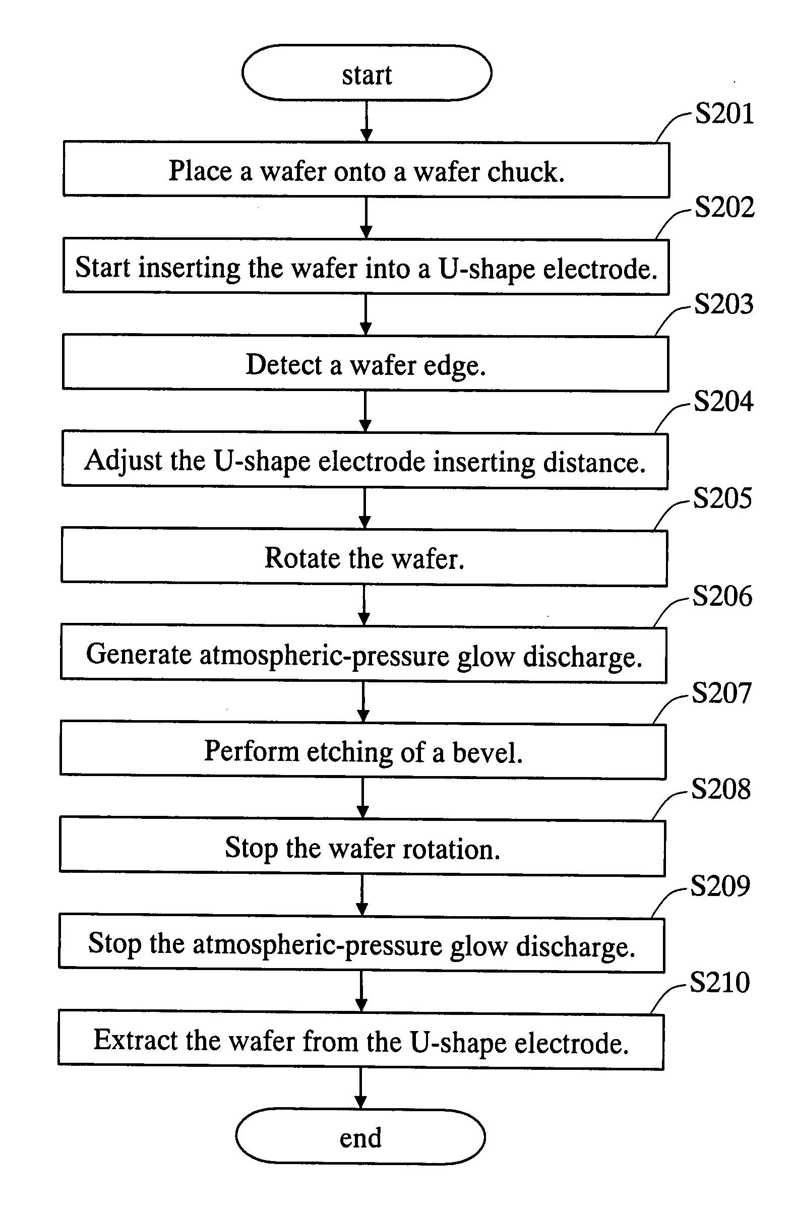
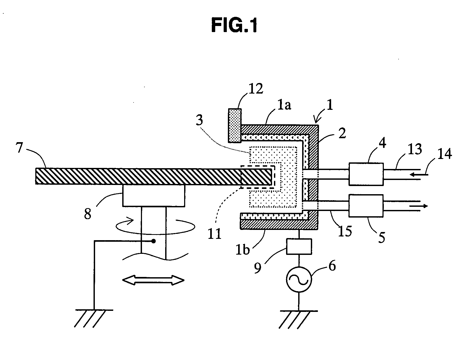
[0027]FIG. 1 is a schematic view of a bevel etching apparatus relating to the first embodiment of the present invention. As shown in FIG. 1, the bevel etching apparatus of the present embodiment is provided with a wafer chuck 8 (a support unit) for supporting a semiconductor substrate 7 (hereafter, referred to as a wafer 7). The wafer chuck 8 is made from a conductor material, such as metal, and ground potential is applied. Further, a surface of the wafer chuck 8 for the placement of the wafer 7 has a diameter which is smaller than that of the wafer 7. A vacuum chuck or an electrostatic chuck is arranged on the contract surface of the wafer chuck 8, and the wafer 7 is attached and secured. Further, the wafer chuck 8 is constructed to be rotatable along the circumferential direction of the wafer 7, by an un-shown drive mechanism.

[0028]Further, the present bevel etching apparatus is provided with an electrode 1 to etch a bevel 11 in the wafer 7 supported by the wafer chuck 8, in which...

second embodiment

[0039]Next, the bevel etching apparatus relating to the Second Embodiment of the present invention is described. FIG. 3 is a schematic view of the bevel etching apparatus relating to the second embodiment of the present invention. The bevel etching of the present embodiment is provided with an electrode 20, which is electrically separated into a front surface side electrode 20a and a rear surface side electrode 20b, instead of the electrode 1 as in the first embodiment. The cross section of the front surface side electrode 20a and the rear surface side electrode 20b is L-shaped, respectively, and both electrodes are arranged to have a roughly U-shape of cross section together. Further, in the present embodiment, the high-frequency power source 6 is connected to the rear surface side electrode 20b, and the ground potential is applied to the front surface side electrode 20a. Furthermore, the dielectric 2 is arranged in the inner wall of the electrode 20 and on the surface of the divid...


PUM

PropertyMeasurementUnit
distanceaaaaaaaaaa
distanceaaaaaaaaaa
frequencyaaaaaaaaaa

Abstract

In the bevel etching apparatus relating to the present invention, a substrate is inserted between electrically connected electrodes. A high-frequency power source is connected to the electrodes, and ground potential is applied to a support unit that supports the substrate. Gas (atmosphere) is supplied to the gap between the electrodes and the application of the high-frequency electric power to the electrodes causes the generation of atmospheric-pressure glow discharge between the electrode and the substrate. Bevel etching is performed by rotating the substrate along the circumferential direction in this condition. According to this construction, the bevel etching can be simultaneously performed to the front surface, the rear surface and the side of the substrate without causing any configuration change in the substrate.

Description

CROSS-REFERENCE TO RELATED APPLICATION[0001]The present application claims the benefit of patent application number 2006-125936, filed in Japan on Apr. 28, 2006, the subject matter of which is incorporated herein by reference.BACKGROUND OF THE INVENTION[0002]1. Field of the Invention[0003]The present invention relates to a bevel etching apparatus and a bevel etching method for etching a region at a predetermined distance from an outer edge of substrate.[0004]2. Description of the Related Art[0005]Conventionally, in a manufacturing process for semiconductor devices, a thin film, such as a conductor or an insulator, is formed on the surface of a semiconductor substrate, on which pattern transfer is performed. At this time, when the pattern transfer is performed even to a substrate periphery (a bevel), a pattern may become separated from the semiconductor substrate and may become particles. This is because the pattern is easily peeled off at the bevel. When these particles are re-depos...

Claims


Application Information

Patent Timeline
Patent Type & Authority Applications(United States)
IPC IPC(8): C03C25/68G01L21/30
CPCH01J37/32018H01J37/32348H01L21/02087H01J37/32825H01J37/32366H01L21/3065
Inventor IMAI, SHIN-ICHI
Owner PANASONIC CORP
Why Eureka
Try Eureka