Transistor having an embedded tensile strain layer with reduced offset to the gate electrode and a method for forming the same

a technology of tensile strain layer and gate electrode, which is applied in the direction of transistors, solid-state diffusion coatings, coatings, etc., can solve the problems of reduced controllability of channels, reduced transistor dimensions, and difficult integration of embedded silicon/carbon layers in drain and source regions, etc., to suppress any dopant diffusion, increase the strain, and high flexibility

Active Publication Date: 2007-11-01
GLOBALFOUNDRIES US INC
View PDF7 Cites 71 Cited by
  • Summary
  • Abstract
  • Description
  • Claims
  • Application Information

AI Technical Summary

Benefits of technology

[0011]Generally, the present invention is directed to a technique for forming silicon-based transistors including a strained silicon carbon material in the drain and source region in order to provide increased strain in the respective channel regions. The silicon/carbon material may be formed on the basis of an implantation process, thereby substantially avoiding the problems involved in selective epitaxial growth techniques used in conventional processes. Due to the incorporation of carbon material by ion implantation, a high degree of flexibility is achieved, in particular in combination with the formation of corresponding transistor elements including strained silicon/germanium material, since the carbon material may be implanted at any appropriate manufacturing stage while the respective P-channel transis...

Problems solved by technology

The continuing shrinkage of the transistor dimensions, however, involves a plurality of issues associated therewith, such as reduced controllability of the channel, also referred to as short channel effects, and the like, that have to be addressed so as to not unduly offset the advantages obtained by steadily decreasing the channel length of MOS transistors.
In contrast to the former approach, the integration of an embedded silicon/carbon layer in the drain and source regions...

Method used


Image

  • Transistor having an embedded tensile strain layer with reduced offset to the gate electrode and a method for forming the same
  • Transistor having an embedded tensile strain layer with reduced offset to the gate electrode and a method for forming the same
  • Transistor having an embedded tensile strain layer with reduced offset to the gate electrode and a method for forming the same

Examples


Embodiment Construction

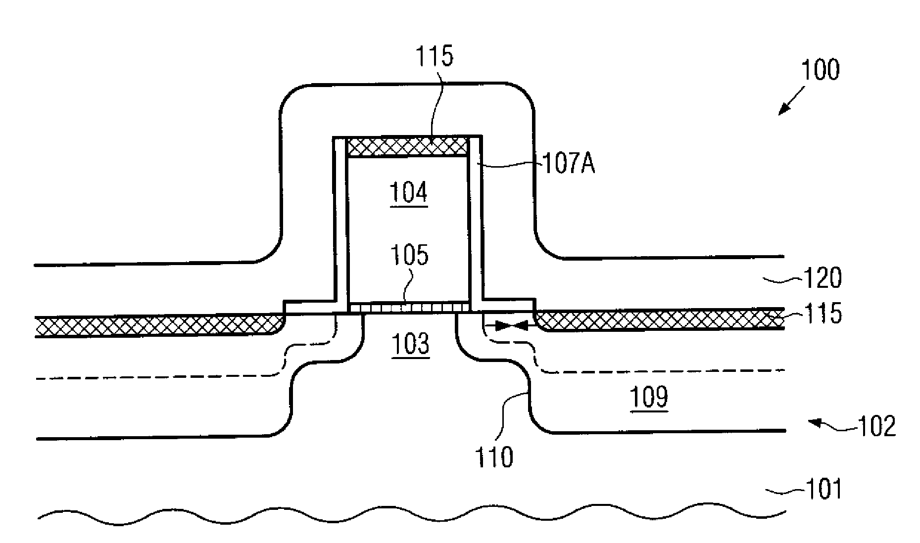
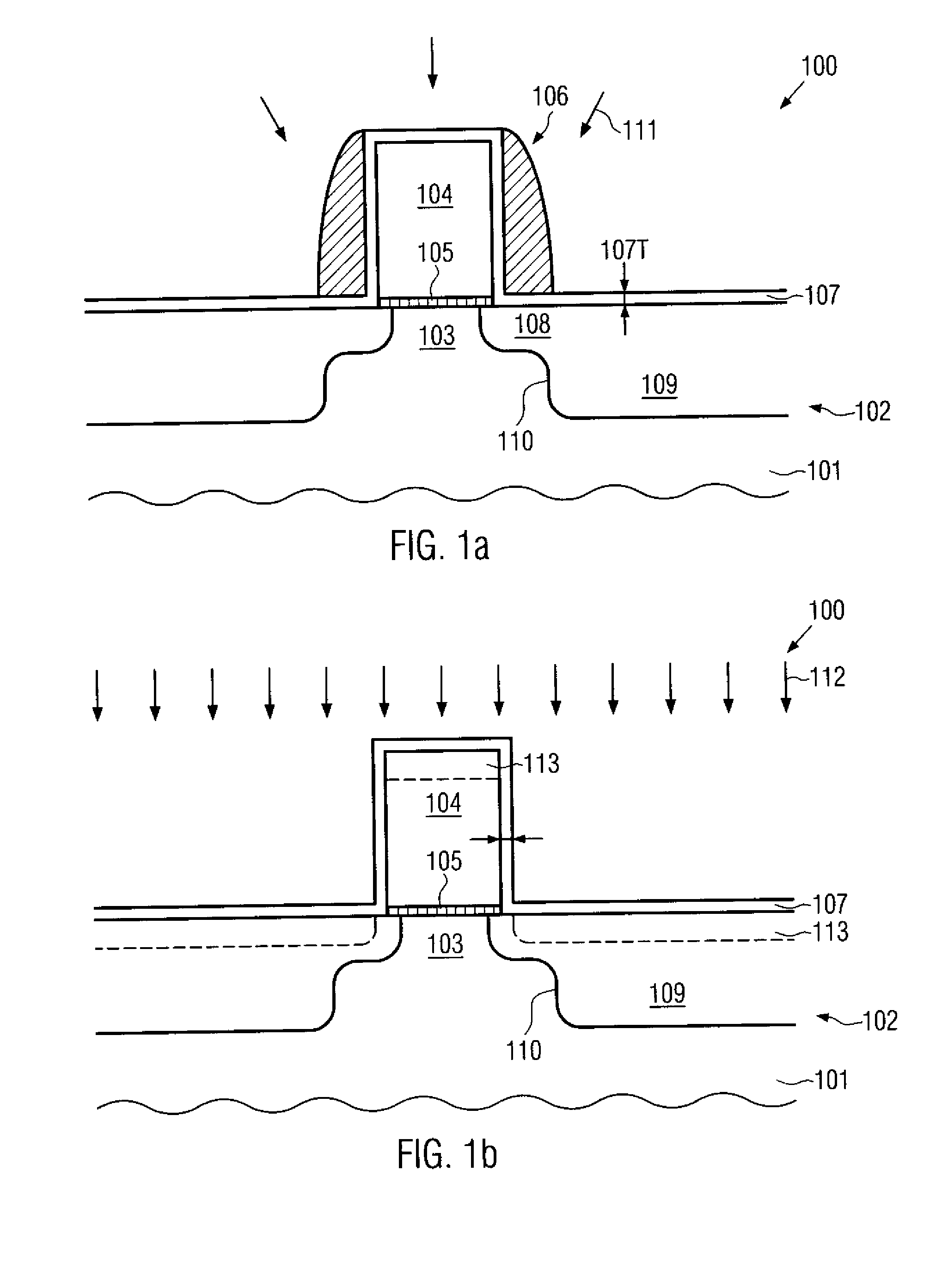
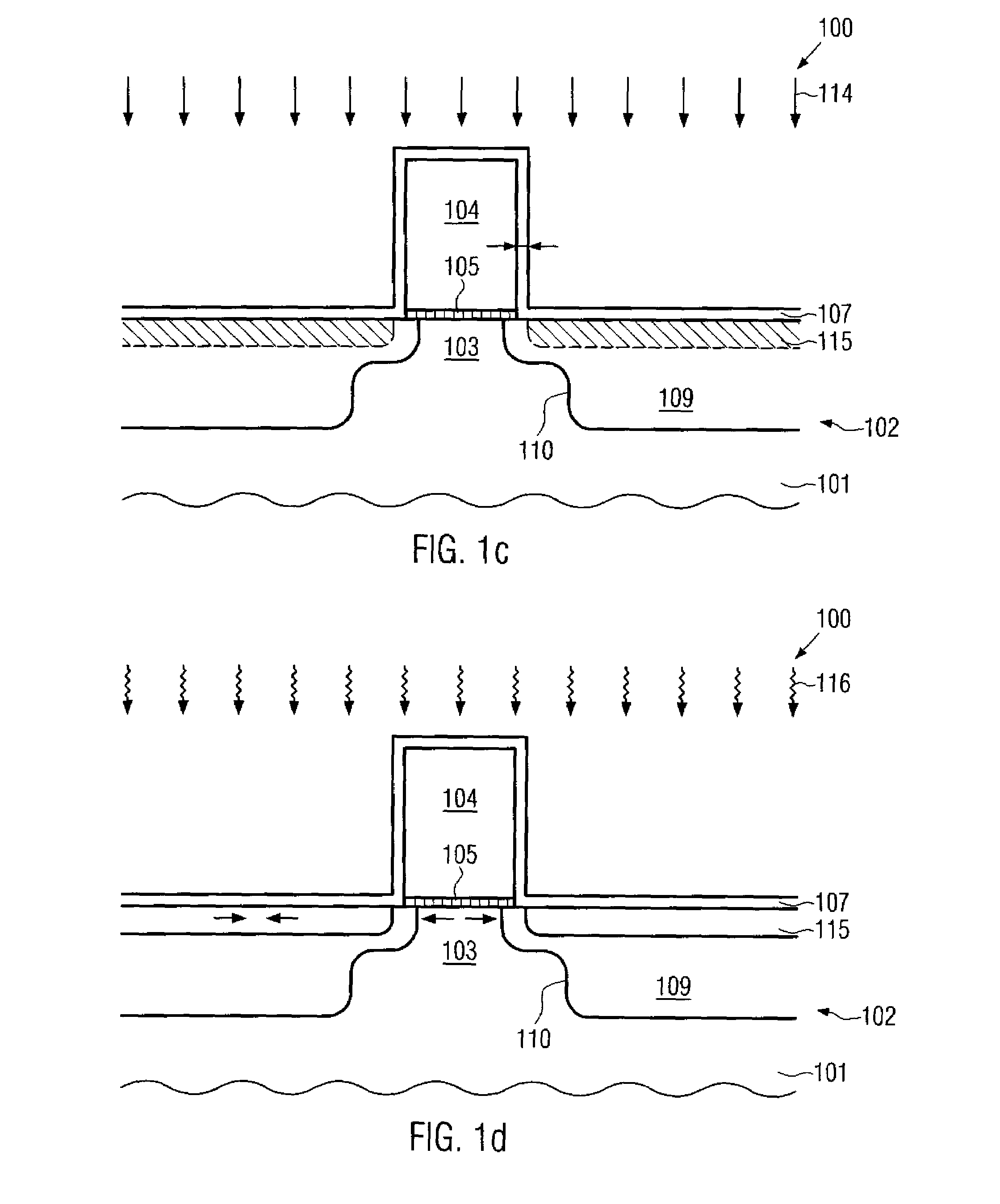
[0020]Illustrative embodiments of the invention are described below. In the interest of clarity, not all features of an actual implementation are described in this specification. It will of course be appreciated that in the development of any such actual embodiment, numerous implementation-specific decisions must be made to achieve the developers' specific goals, such as compliance with system-related and business-related constraints, which will vary from one implementation to another. Moreover, it will be appreciated that such a development effort might be complex and time-consuming, but would nevertheless be a routine undertaking for those of ordinary skill in the art having the benefit of this disclosure.

[0021]The present invention will now be described with reference to the attached figures. Various structures, systems and devices are schematically depicted in the drawings for purposes of explanation only and so as to not obscure the present invention with details that are well ...


PUM

PropertyMeasurementUnit
Percent by atomaaaaaaaaaa
Electrical conductivityaaaaaaaaaa
Concentrationaaaaaaaaaa

Abstract

By incorporating carbon by means of ion implantation and a subsequent flash-based or laser-based anneal process, strained silicon/carbon material with tensile strain may be positioned in close proximity to the channel region, thereby enhancing the strain-inducing mechanism. The carbon implantation may be preceded by a pre-amorphization implantation, for instance on the basis of silicon. Moreover, by removing a spacer structure used for forming deep drain and source regions, the degree of lateral offset of the strained silicon/carbon material with respect to the gate electrode may be determined substantially independently from other process requirements. Moreover, an additional sidewall spacer used for forming metal silicide regions may be provided with reduced permittivity, thereby additionally contributing to an overall performance enhancement.

Description

BACKGROUND OF THE INVENTION[0001]1. Field of the Invention[0002]Generally, the present invention relates to the formation of integrated circuits, and, more particularly, to the formation of transistors having strained channel regions by using an embedded strained layer in the drain and source regions to enhance charge carrier mobility in the channel region of a MOS transistor.[0003]2. Description of the Related Art[0004]The fabrication of integrated circuits requires the formation of a large number of circuit elements on a given chip area according to a specified circuit layout. Generally, a plurality of process technologies are currently practiced, wherein, for complex circuitry, such as microprocessors, storage chips and the like, CMOS technology is currently one of the most promising approaches, due to the superior characteristics in view of operating speed and / or power consumption and / or cost efficiency. During the fabrication of complex integrated circuits using CMOS technology...

Claims


Application Information

Patent Timeline
IPC IPC(8): H01L21/425
CPCC23C8/20C23C8/80H01L21/823807H01L21/823814H01L29/7848H01L29/6653H01L29/6659H01L29/7833H01L29/7843H01L29/665
Inventor WEI, ANDYKAMMLER, THORSTENHOENTSCHEL, JANHORSTMANN, MANFRED
Owner GLOBALFOUNDRIES US INC
Why Eureka
Try Eureka