
Electro-optical device and electronic apparatus

a technology of optical devices and electronic devices, applied in electrical devices, semiconductor devices, instruments, etc., can solve the problems of reduced dielectric strength or dielectric breakdown, inability to uniformly generate electric fields across, and reduced dielectric strength, so as to reduce thickness and reduce dielectric strength

Active Publication Date: 2007-11-15
JAPAN DISPLAY WEST
View PDF3 Cites 23 Cited by
  • Summary
  • Abstract
  • Description
  • Claims
  • Application Information

AI Technical Summary

Benefits of technology

[0011]An advantage of a aspect of the invention is to provide an electro-optical device in which even if dielectric layers of storage capacitors have a reduced thickness, regions overlapping with upper electrodes and end portions of lower electrodes can be prevented from being reduced in dielectric strength. An advantage of another aspect of the invention is to provide an electronic apparatus including the electro-optical device.
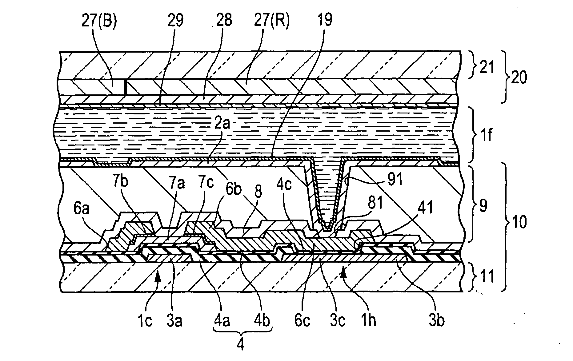
[0013]Since the thin portions are located in the inner portions of the regions overlapping with the lower and upper electrodes, the storage capacitors have high capacitance per unit area. Dielectric layers of the storage capacitors have a small thickness and the thick portions of the gate insulating layer are located in the regions overlapping with the upper electrodes and the end portions of the lower electrodes. Hence, electric field concentration due to stepped portions can be mitigated by the thick portions of the gate insulating layer and therefore the dielectric strength of the end portions of the lower electrodes is prevented from being reduced. Even if electric fields are concentrated on portions of the dielectric layers that are located between the upper electrodes and the end portions of the lower electrodes because the dielectric layers have a stepped shape due to the stepped portions corresponding to the end portions of the lower electrodes, dielectric breakdown does not occur because the portions of the dielectric layers have a large thickness. Even if portions of the dielectric layers that cover the end portions of the lower electrodes are nonuniform because the growth direction and the deposition rate of the gate insulating layer depend on the morphology of components disposed under the gate insulating layer, neither a reduction in dielectric strength nor dielectric breakdown (short circuits) occurs because these portions of the dielectric layers have a large thickness. A reduction in the thickness of the dielectric layers will cause the above problems. According to the present invention, although the dielectric layers have a small thickness, the problems can be prevented. That is, although the thickness of the dielectric layers is reduced such that the storage capacitors have increased capacitance per unit area, the storage capacitors can be formed so as to have high dielectric strength.
[0015]In the electro-optical device, the thin portions are preferably located outside the regions overlapping with the upper electrodes and the end portions of the lower electrodes. This allows the thin portions to have an increased area; hence, the storage capacitors have increased capacitance per unit area. In regions other than the regions overlapping with the upper electrodes and the end portions of the lower electrodes, electric field concentration due to the stepped portions and the deterioration of film quality do not occur at the end portions of the upper electrodes and therefore the dielectric strength of the storage capacitors is not reduced.
[0016]In the electro-optical device, the thick portions preferably extend inward from the end portions of the electrolytic solution and have a width greater than the thickness of the thick portions. If conditions are set as described above, electric field concentration due to the stepped portions and a reduction in dielectric strength due to the deterioration of film quality can be prevented. If the thin portions are expanded within a range satisfying such conditions, the capacitance per unit area of the storage capacitors can be increased.
[0017]In the electro-optical device, it is preferable that the gate insulating layer include a lower gate insulating sublayer including one or more insulating layer sections and a upper gate insulating sublayer including one or more insulating layer sections, the thin portions be formed by partly removing the lower gate insulating sublayer, and the thick portions correspond to portions in which the upper gate insulating sublayer is disposed on the lower gate insulating sublayer. According to this configuration, the upper gate insulating sublayer and the semiconductor layers can be continuously formed; hence, the interfaces between the upper gate insulating sublayer and the semiconductor layers can be maintained clean. This enhances the reliability of the thin-film transistors. The thin portions of the gate insulating layer are used as the dielectric layers of the storage capacitors, that is, the dielectric layers include no portions of the lower gate insulating sublayer but portions of the upper gate insulating sublayer 4b; hence, the gate insulating layer need not be partly removed in the thickness direction thereof by etching. This prevents the capacitance of the storage capacitors from being varied due to differences in etching depth. Since the lower gate insulating sublayer is partly removed and the upper gate insulating sublayer is used to form the dielectric layers of the storage capacitors, the upper gate insulating sublayer is not exposed to static electricity or plasma when the lower gate insulating sublayer is partly removed by dry etching. This protects the upper gate insulating sublayer from surface damage or defects. The upper gate insulating sublayer is not in contact with an etching solution for etching the lower gate insulating sublayer; hence, no pinholes are formed in the upper gate insulating sublayer. This prevents the reduction of the dielectric strength of the storage capacitors.

Problems solved by technology

Therefore, when voltages are applied between the lower and upper electrodes, electric fields cannot be uniformly generated across the dielectric layers and therefore are concentrated on the end portions of the lower electrodes.
This causes a reduction in dielectric strength or dielectric breakdown (short circuits).
A reduction in the thickness of the dielectric layers will cause the above problems.

Method used


Image

  • Electro-optical device and electronic apparatus
  • Electro-optical device and electronic apparatus
  • Electro-optical device and electronic apparatus

Examples


first embodiment

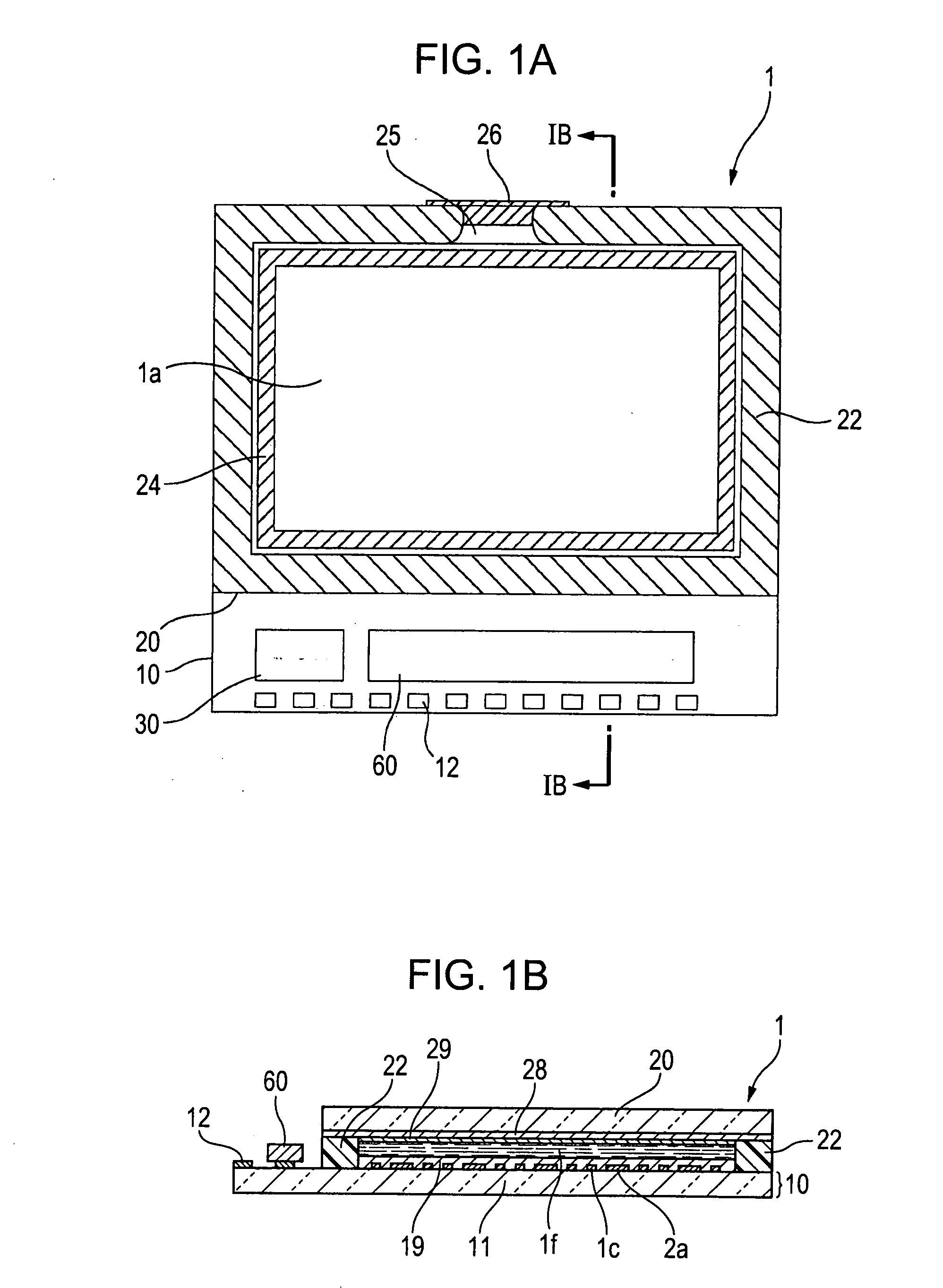
[0039]An electro-optical device 1 according to a first embodiment of the present invention will now be described. FIG. 1A shows the electro-optical device 1 in plan view and FIG. 1B shows the electro-optical device 1 in sectional view taken along the line IB-IB of FIG. 1A. The electro-optical device 1 is a transmissive active matrix liquid crystal device operating in a twisted nematic (TN) mode, an electrically controlled birefringence (ECB) mode, or a vertical aligned nematic (VAN) mode. The electro-optical device 1 includes an element substrate 10 and a counter substrate 20 that is bonded to the element substrate 10 with a sealing member 22 disposed therebetween. A liquid crystal 1f is held between the element and counter substrates 10 and 20. The element substrate 10 has an end region located outside of the sealing member 22. A data line-driving integrated circuit (IC) 60 and a scanning line-driving IC 30 are mounted on the end region of the element substrate 10 by a chip-on-glas...

second embodiment

[0079]FIG. 8A shows one of pixels 1b disposed in an electro-optical device 1 according to a second embodiment of the present invention in plan view and FIG. 8B shows the pixel 1b in sectional view taken along the line VIIIB-VIIIB of FIG. 8A. FIG. 9A shows one of storage capacitors 1h disposed in the electro-optical device 1 shown in FIG. 8 in plan view in an enlarged manner, FIG. 9B shows one of regions overlapping with end portions of lower electrodes 3c and upper electrodes 6c in sectional view in an enlarged manner, and FIG. 9C shows one of regions overlapping with the lower electrodes 3c and end portions of the upper electrodes 6c in sectional view in an enlarged manner. With reference to FIG. 8A, pixel electrodes 2a are shown by thick broken lines, gate lines 3a and thin-films formed together therewith are shown by thin solid lines, source lines 6a and thin-films formed together therewith are shown by thin dotted-chain lines, and semiconductor layers 7a are shown by thin dotted...

third embodiment

[0088]FIG. 11A shows one of pixels 1b disposed in an electro-optical device 1 according to a third embodiment of the present invention in plan view and FIG. 11B shows the pixel 1b in sectional view taken along the line XIB-XIB of FIG. 11A. With reference to FIG. 11A, pixel electrodes 2a are shown by thick broken lines, gate lines 3a and thin-films formed together therewith are shown by thin solid lines, source lines 6a and thin-films formed together therewith are shown by thin dotted-chain lines, and semiconductor layers 7a are shown by thin dotted lines. Furthermore, dielectric layers 4c of storage capacitors 1h that are thin portions of a gate insulating layer 4 are shown by thick solid lines and contact holes as well as the gate lines 3a are shown by thin solid lines. The electro-optical device 1 of this embodiment has substantially the same configuration as that of the electro-optical device 1 of the first embodiment; hence, components common to these devices have the same refer...


PUM


Abstract

An electro-optical device includes an element substrate having a plurality of pixel regions; thin-film transistors, arranged in the pixel regions, including gate electrodes, portions of a gate insulating layer, and semiconductor layers; pixel electrodes electrically connected to drain regions of the thin-film transistors; and storage capacitors including lower electrodes and upper electrodes that are opposed to the lower electrodes with insulating layers disposed therebetween, the insulating layers being made of the same material as that for forming the gate insulating layer. The upper electrodes overlap with some of end portions of the lower electrodes. The gate insulating layer has thin portions located in inner portions of regions overlapping with the lower and upper electrodes and thick portions which are located in regions overlapping with the upper electrodes and the end portions of the lower electrodes and which have a thickness greater than that of the thin portions.

Description

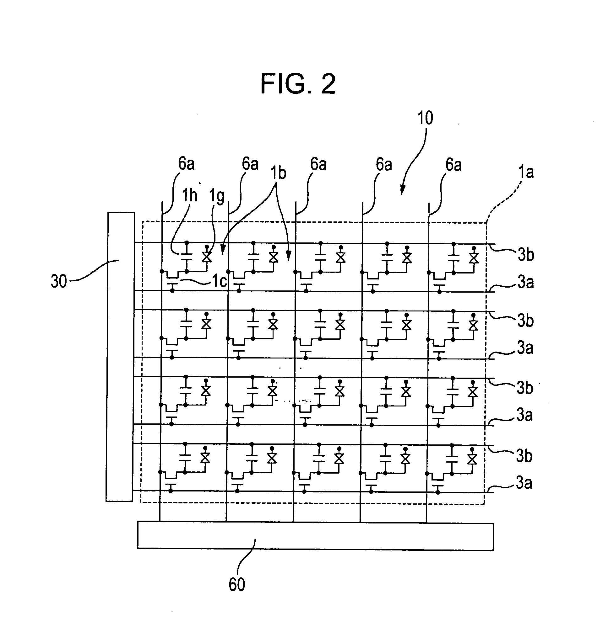
BACKGROUND[0001]1. Technical Field[0002]The present invention relates to an electro-optical device including thin-film transistors and storage capacitors arranged above an element substrate and an electronic apparatus including the electro-optical device.[0003]2. Related Art[0004]Among various electro-optical devices is an active matrix-type liquid crystal device. In the liquid crystal device, a liquid crystal is held between an element substrate 10 shown in FIGS. 16A and 16B and a counter substrate (not shown). The element substrate 10 includes a plurality of pixel regions 1e corresponding to intersections of gate lines 3a (scanning lines) and source lines 6a (date lines). The pixel regions 1e include thin-film transistors 1c for switching pixels and pixel electrodes 2a electrically connected to drain regions 6b of the thin-film transistors 1c. The alignment of the liquid crystal is controlled for each pixel in such a manner that image signals are applied to the pixel electrodes 2a...

Claims


Application Information

Patent Timeline
IPC IPC(8): H01L29/76H01L29/745
CPCG02F1/136213G02F2201/40H01L27/1255G02F2202/42G02F2202/103G02F1/136
Inventor HIRABAYASHI, YUKIYASATO, TAKASHI
Owner JAPAN DISPLAY WEST
Learn More