Ultrashort laser pulse wafer scribing

a laser pulse and ultrashort technology, applied in the field of laser cutting or scribing, can solve the problems of lack of mechanical strength, low k dielectric material very sensitive to stress, and conventional mechanical and laser cutting methods are not well suited for scribing many advanced finished wafers, etc., to achieve the effect of reducing or no mechanical and/or thermal stress, and reducing or no debris

Inactive Publication Date: 2007-11-29
ELECTRO SCI IND INC
View PDF32 Cites 93 Cited by
  • Summary
  • Abstract
  • Description
  • Claims
  • Application Information

AI Technical Summary

Benefits of technology

[0008]The embodiments disclosed herein provide systems and methods of scribing a finished wafer that includes low-k dielectric and / or other materials as fast as or faster than existing mechanical and / or laser methods. However, the laser scribing is performed with reduced or no mechanical and / or thermal stress and with reduced or no debris. Thus, little or no post process cleaning is required. Further, clean, straight edge cuts are produced with no additional lateral separation of the devices on wafer required to accommodate the scribing process.

Problems solved by technology

However, conventional mechanical and laser cutting methods are not well suited for scribing many advanced finished wafers with, for example, low-K dielectric materials.
Relatively low density, lack of mechanical strength and sensitivity to thermal stress make low-k dielectric material very sensitive to stress.
Conventional mechanical wafer dicing and scribing techniques are known to cause chips, cracks and other types of defects in low-k materials, thus damaging the IC devices.
However, this severely reduces throughput.
Further, known laser techniques can produce excessive heat and debris.
However, these long pulse widths allow excessive heat diffusion that causes heat affected zones, recast oxide layers, excessive debris and other problems.
Thus, reliability and yield are reduced.
In addition, conventional laser cutting profiles may suffer from trench backfill of laser ejected material.
When the wafer thickness is increased, this backfill becomes more severe and reduces dicing speed.
Further, for some materials under many process conditions, the ejected backfill material may be more difficult to remove on subsequent passes than the original target material.
Thus, cuts of low quality are created that can damage IC devices and require additional cleaning and / or wide separation of the devices on the substrate.

Method used


Image

  • Ultrashort laser pulse wafer scribing
  • Ultrashort laser pulse wafer scribing
  • Ultrashort laser pulse wafer scribing

Examples


Embodiment Construction

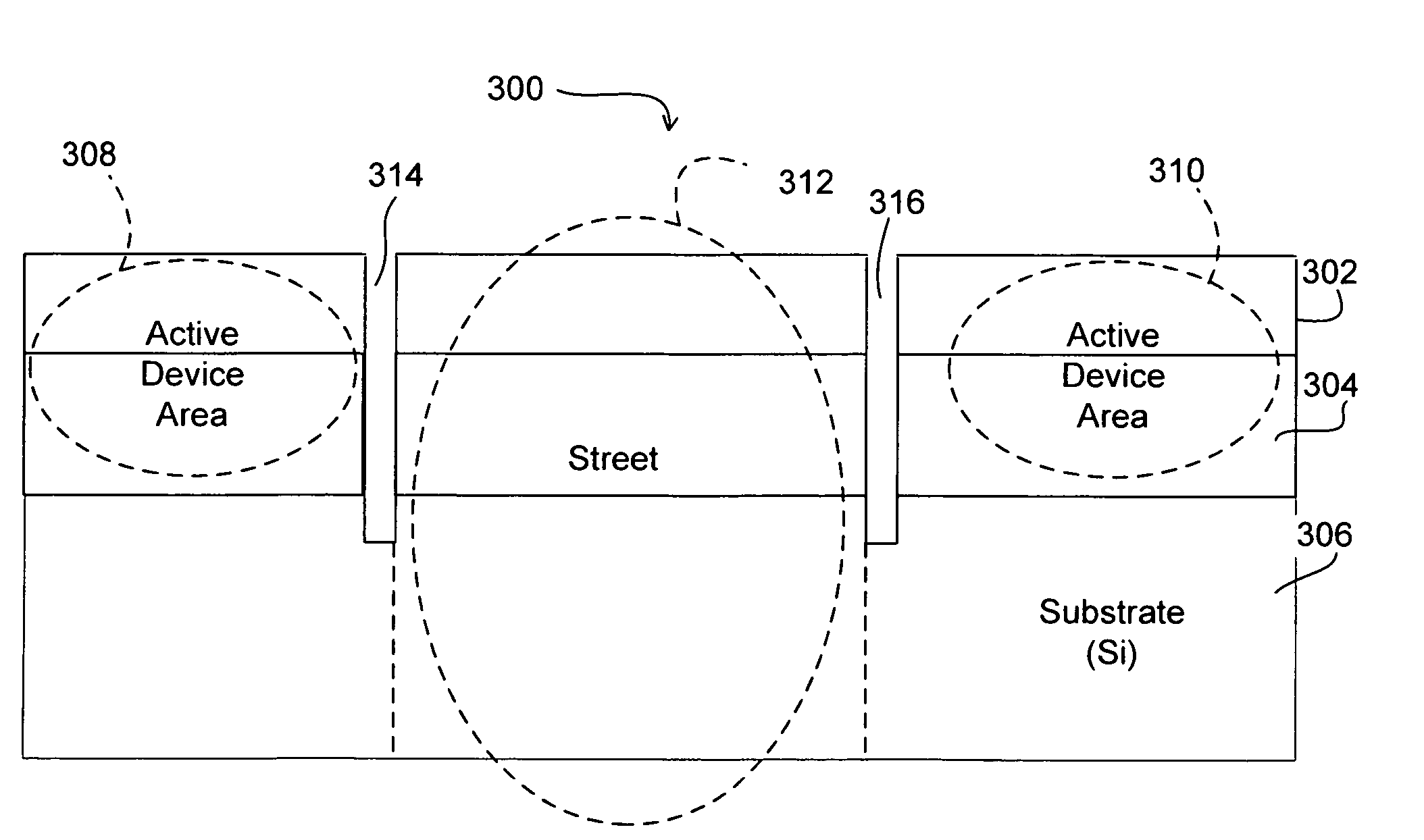
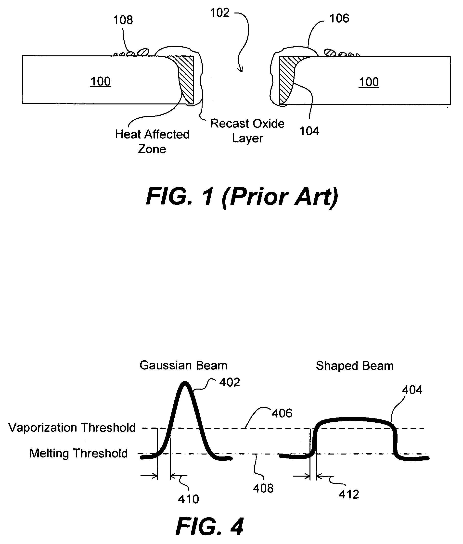
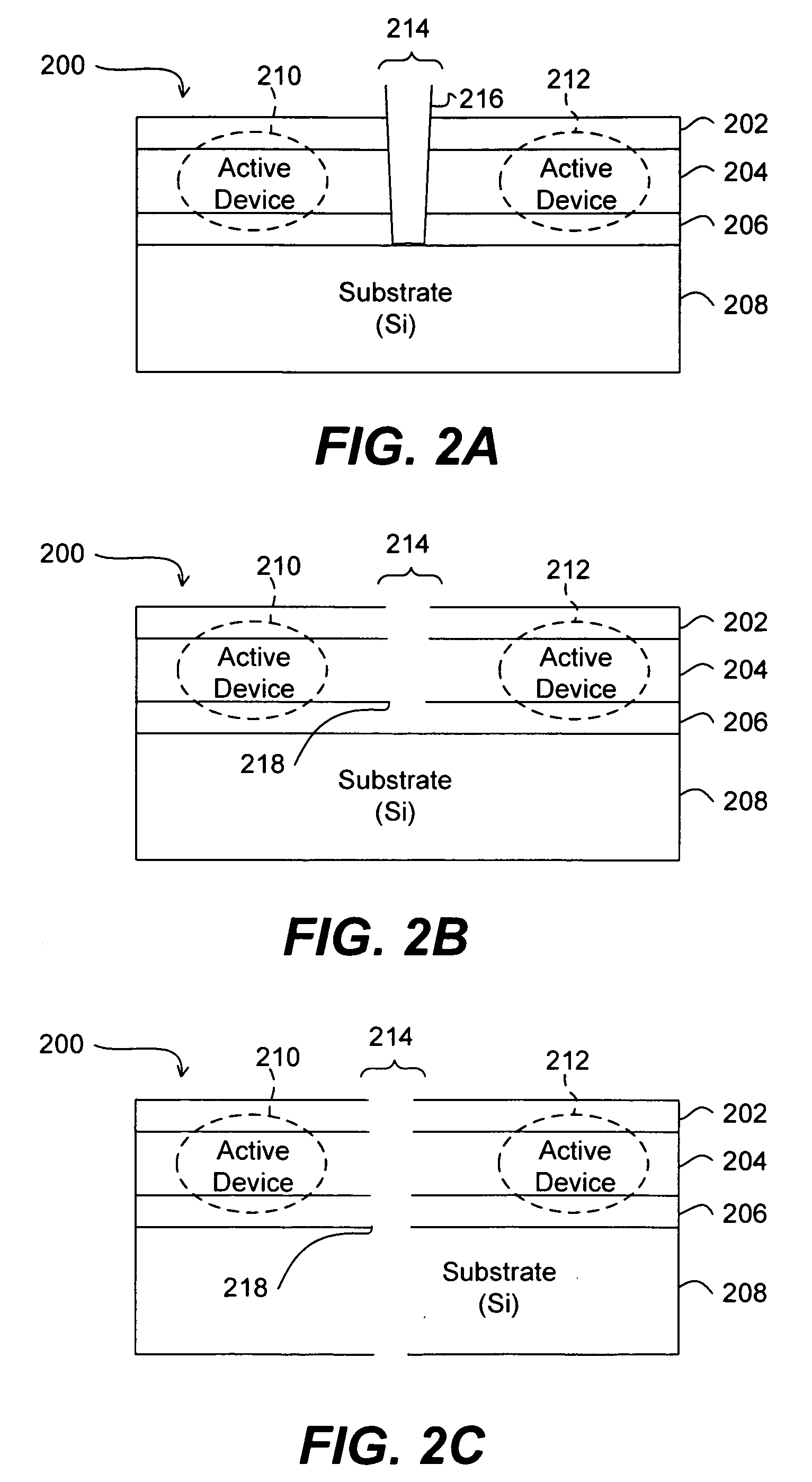
[0026]The ability of a material to absorb laser energy determines the depth to which that energy can perform ablation. Ablation depth is determined by the absorption depth of the material and the heat of vaporization of the material. Parameters such as wavelength, pulse width duration, pulse repetition frequency, and beam quality can be controlled to improve cutting speed and the quality of the cut surface or kerf. In one embodiment, one or more of these parameters are selected so as to provide a substantially low fluence (typically measured in J / cm2) that has just enough energy to ablate the target material. Thus, the amount of excessive energy deposited into the material is reduced or eliminated. Using a lower fluence reduces or eliminates recast oxide layers, heat affected zones, chipping, cracking, and debris. Thus, die break strength is increased and the amount of post-laser cleaning required is decreased.

[0027]U.S. Pat. No. 5,656,186 to Mourou et al. teaches that the ablation ...


PUM

PropertyMeasurementUnit
energyaaaaaaaaaa
energyaaaaaaaaaa
average poweraaaaaaaaaa

Abstract

Systems and methods are provided for scribing wafers with short laser pulses so as to reduce the ablation threshold of target material. In a stack of material layers, a minimum laser ablation threshold based on laser pulse width is determined for each of the layers. The highest of the minimum laser ablation thresholds is selected and a beam of one or more laser pulses is generated having a fluence in a range between the selected laser ablation threshold and approximately ten times the selected laser ablation threshold. In one embodiment, a laser pulse width in a range of approximately 0.1 picosecond to approximately 1000 picoseconds is used. In addition, or in other embodiments, a high pulse repetition frequency is selected to increase the scribing speed. In one embodiment, the pulse repetition frequency is in a range between approximately 100 kHz and approximately 100 MHz.

Description

TECHNICAL FIELD [0001]This application relates to laser cutting or scribing and, in particular, to a method of manufacturing integrated circuitry using ultrashort laser pulses at a high repetition rate to ablate material.BACKGROUND INFORMATION [0002]Integrated circuits (ICs) are generally fabricated in an array on or in a semiconductor substrate. ICs generally include several layers formed over the substrate. One or more of the layers may be removed along scribing lanes or streets using a mechanical saw or a laser. After scribing, the substrate may be throughout, sometimes called diced, using a saw or laser to separate the circuit components from one another.[0003]Semiconductor manufacturers have been shrinking transistor sizes in ICs to improve chip performance. This has resulted in increased speed and device density. To facilitate further improvements, semiconductor manufacturers use materials to reduce the capacitance of dielectric layers. For example, to form a finer circuit pat...

Claims


Application Information

Patent Timeline
Patent Type & Authority Applications(United States)
IPC IPC(8): B23K26/38B23K26/40
CPCB23K26/0635B23K26/383B23K26/385B23K26/367B23K26/4075B23K2201/40B23K26/386B23K26/0624B23K26/384B23K26/40B23K26/389B23K2103/50B23K2101/40B23K26/364H01L21/324H01L21/30
Inventor ALBELO, JEFFREY A.PIROGOVSKY, PETER
Owner ELECTRO SCI IND INC
Why Eureka
Try Eureka