Process including silo-chloro passivation for etching tungsten silicide overlying polysilicon

a technology of tungsten silicide and etching process, which is applied in the field ofplasma etching, can solve the problems of increasing difficulties, severe etching process requirements, and shrinkage, and achieve the effects of reducing the depth microloading, reducing the residence time of etching, and increasing the selectivity of silicon

Inactive Publication Date: 2007-12-06
APPLIED MATERIALS INC
View PDF23 Cites 7 Cited by
  • Summary
  • Abstract
  • Description
  • Claims
  • Application Information

AI Technical Summary

Benefits of technology

[0013]The principal etchant for the tungsten is gas containing both chlorine and fluorine, for example, NF3 and Cl2. Low wafer biasing, for example, less than one-third that of the source power, reduces depth microloading.
[0014]Addition of an oxidizing gas, for example, both oxygen and nitrogen, increases selectivity to silicon.
[0015]Addition of argon or helium, particularly in the main etch, reduces the residence time for etch byproducts and prevents undercutting of the tungsten material.
[0016]Decreasing the NF3 / Cl2 ratio in the over etch improves selectivity and reduces undercutting.
[0017]Silicon tetrachloride may be added for a further increase in selectivity.

Problems solved by technology

The shrinkage has introduced severe requirements upon the etching process used to form the memory cell, especially the etching of the tungsten-based contact on the polysilicon control gate.
The etching of the tungsten-based contact layer 54, particularly when it is composed of WSi, has presented increasing difficulties as the lateral and vertical dimension shrink with increasingly large flash memories.

Method used


Image

  • Process including silo-chloro passivation for etching tungsten silicide overlying polysilicon
  • Process including silo-chloro passivation for etching tungsten silicide overlying polysilicon
  • Process including silo-chloro passivation for etching tungsten silicide overlying polysilicon

Examples


Embodiment Construction

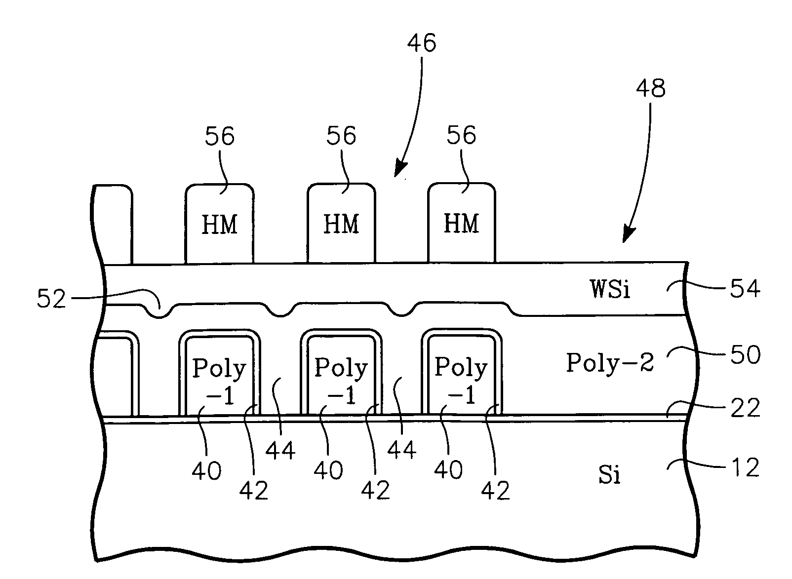
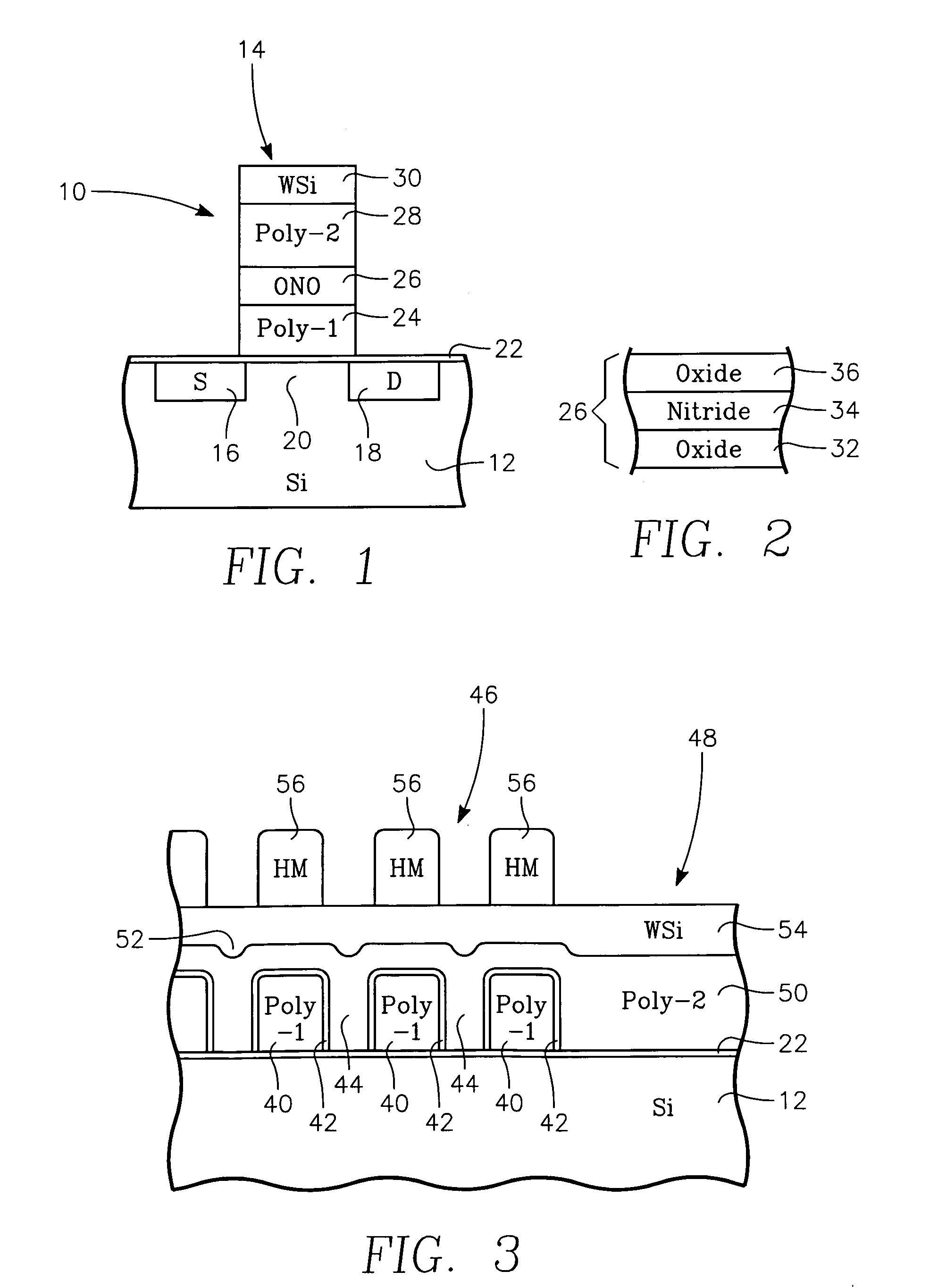
[0024]With reference to FIG. 3, we have observed several difficulties in etching the WSi layer 54 through the hard mask 56. In advanced designs, the thicknesses of all the layers need to minimized to reduce the overall size of the memory cell so there is little margin for errors and non-uniformity in etching depths. The depths of the troughs 52 have been observed to be up to 70% of the thickness of the WSi layer 54 in more planar areas. Accordingly, once a main etch (ME) has etched through the WSi layer 54 in the planar areas, a long over etch (OE) is required to clear out the WSi residue from the troughs 52. The over etch may extend for 75 to 100% of the time of the main etch. The long over etch requires good selectivity of the WSi etch to silicon in the second polysilicon layer 50. The etching profiles need to be maintained as vertical as possible, both in the WSi layer 54 and in the portion of the polysilicon consumed in the overetch. The distinction between the dense and iso are...


PUM

PropertyMeasurementUnit
boiling pointaaaaaaaaaa
melting pointaaaaaaaaaa
thicknessesaaaaaaaaaa

Abstract

A method of plasma etching tungsten silicide over polysilicon particularly useful in fabricating flash memory having both a densely packed area and an open (iso) area requiring a long over etch due to microloading. Wafer biasing is decreased in the over etch. The principal etchant include NF3 and Cl2. Argon is added to prevent undercutting at the dense/iso interface. Oxygen and nitrogen oxidize any exposed silicon to increase etch selectivity and straightens the etch profile. SiCl4 as an example of a silicon and chlorine containing passivating gas may be added for additional selectivity.

Description

RELATED APPLICATION[0001]This application is a division of Ser. No. 11 / 445,709 filed Jun. 2, 2006.FIELD OF THE INVENTION[0002]The invention relates generally to plasma etching. In particular, the invention relates to etching tungsten and other tungsten-containing materials over silicon.BACKGROUND ART[0003]Flash memory has assumed an increasingly important position in semiconductor memory technology. It provides relatively fast non-volatile rewritable memory, which is particularly attractive in mobile applications such as cell phones, portable music players, and other devices which rely upon battery power but are often turned off for extended periods. Nonetheless, flash memory chips are being economically fabricated which have a capacity of greater than a gigabit.[0004]However, large-capacity flash memories of the desired characteristics have been accomplished by aggressively reducing the area of the memory cells, by reducing the thickness of many of the important layers, and by rely...

Claims


Application Information

Patent Timeline
Patent Type & Authority Applications(United States)
IPC IPC(8): C23F1/00H01L21/302
CPCH01L21/28273H01L21/32137H01L21/32136H01L29/40114H01L29/42324
Inventor LEE, KYEONG-TAECHOI, JINHANJANG, BIDESHMUKH, SHASHANK C.SHEN, MEIHUALILL, THORSTEN B.YU, JAE BUM
Owner APPLIED MATERIALS INC
Why Eureka
Try Eureka