

Semiconductor device and method for manufacturing same
a semiconductor and semiconductor technology, applied in the direction of semiconductor devices, semiconductor/solid-state device details, electrical apparatus, etc., can solve the problems of difficult connection through wire bonding, difficult to ensure high-speed signal transmission, and the disadvantage of being inferior to a system-on-chip (soc) in the speed of signal transmission between chips
- Summary
- Abstract
- Description
- Claims
- Application Information
AI Technical Summary
Benefits of technology
Problems solved by technology
Method used
Image

Examples
Embodiment Construction
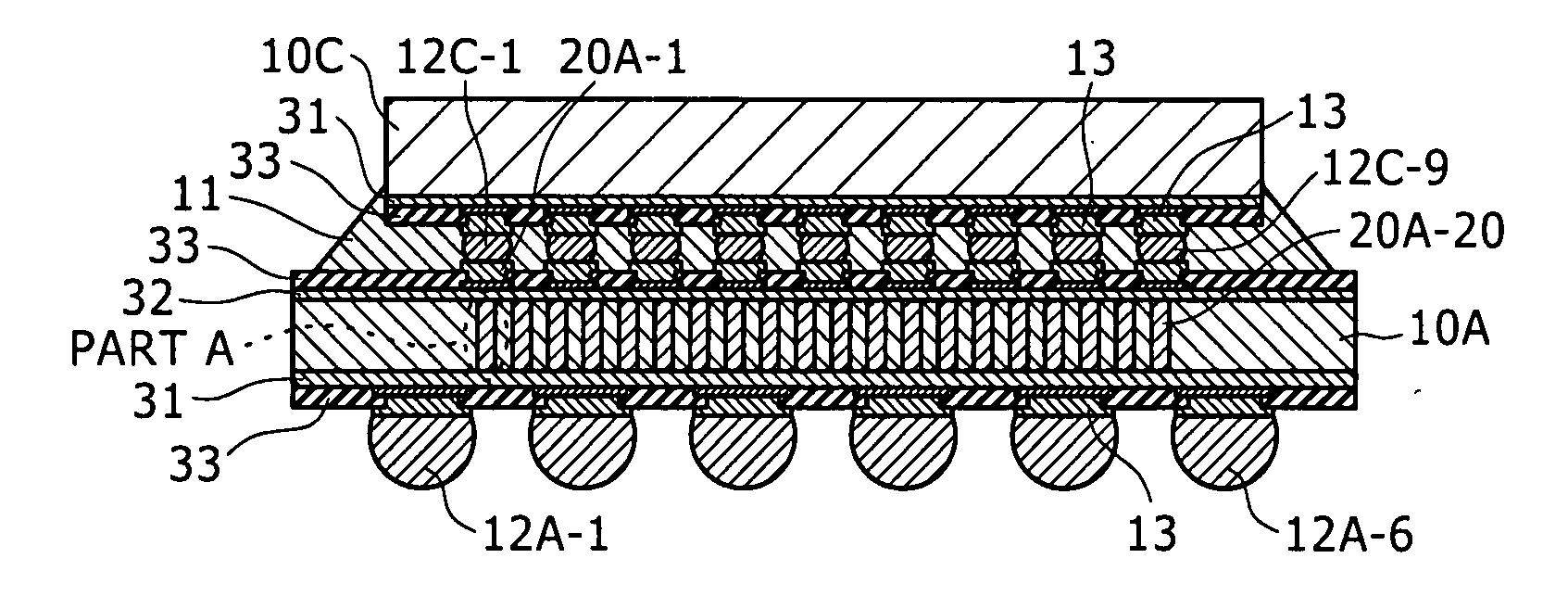
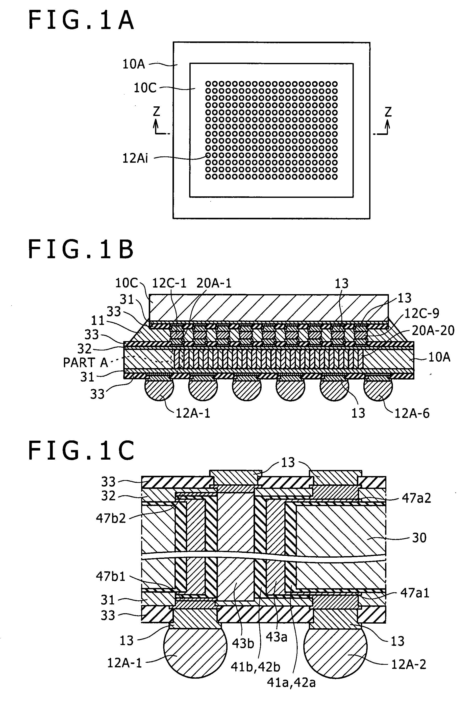
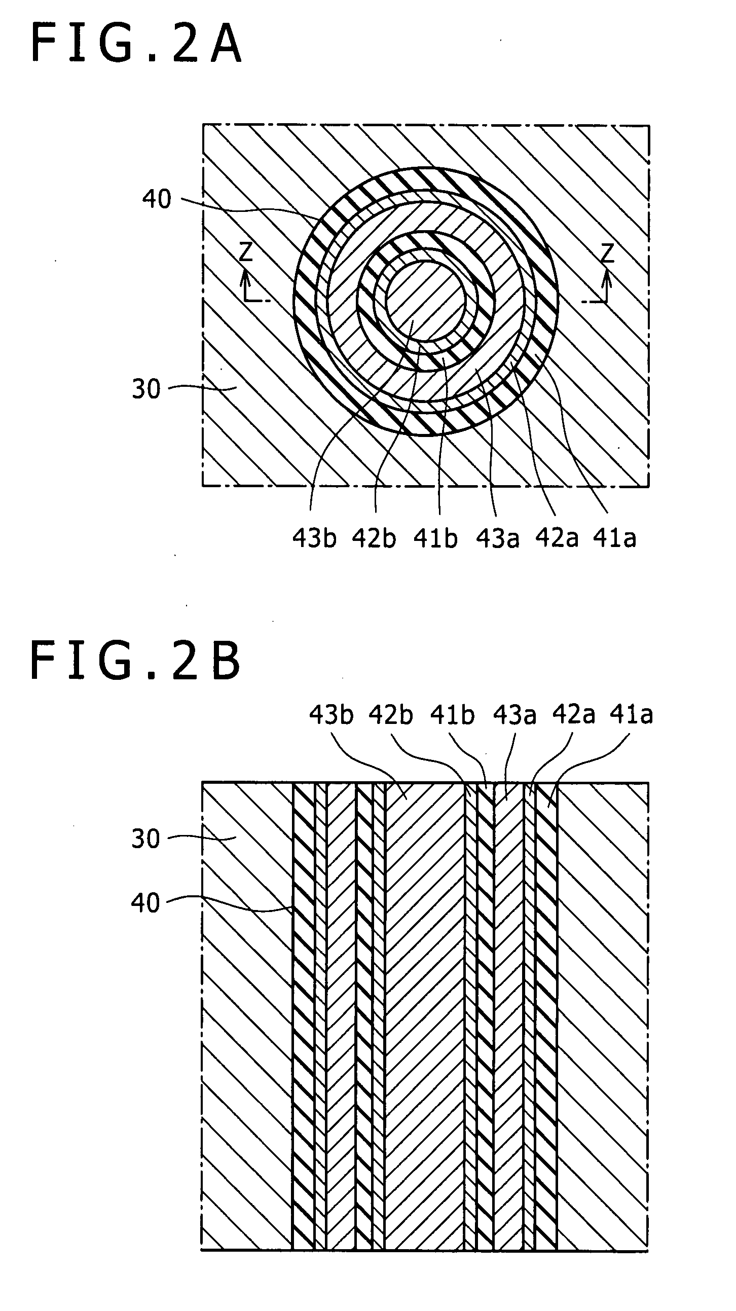
[0110] In a semiconductor device according to an embodiment of the present invention, it is preferable to form in a through-hole an insulating layer for electrically insulating plural through-interconnects from each other. If plural through-interconnects are electrically insulated from each other, the through-interconnects can be used as interconnect lines that transmit signals independently of each other. Furthermore, it is preferable that the plural through-interconnects be concentric with each other. This allows formation of plural through-interconnects having a large sectional area.
[0111] In addition, it is preferable that the through-holes be formed in a peripheral region or an inside region of the peripheral region of the substrate. Because plural through-interconnects are formed in one through-hole, there is no need to form through-holes at a high density, which can suppress a substrate size increase. Even when through-holes are formed in an element-formation region on a sub...
PUM
 Abstract
Description
Claims
Application Information