Structure and method of chemically formed anchored metallic vias

a technology of chemical formation and metallic vias, which is applied in the direction of semiconductor devices, semiconductor/solid-state device details, electrical apparatus, etc., can solve the problems of increasing the number of integrated circuits, new integration challenges, and reducing the efficiency of routing these signals across the device, so as to achieve elimination or significant reduction of the sputter-etching process, the effect of high stress migration

Active Publication Date: 2008-01-17
GLOBALFOUNDRIES US INC
View PDF17 Cites 43 Cited by
  • Summary
  • Abstract
  • Description
  • Claims
  • Application Information

AI Technical Summary

Benefits of technology

[0013] The present invention provides methods that enable the ability to use a less aggressive PVD liner deposition processes, while producing structures known to give a desired high stress migration and electro-migration reliability. The present invention circumvents the issue of sputter damage of low k (on the order of 3.2 or less) dielectrics by creating the via “anchors” (interlocked and interpenetrated vias) through chemical means. This allows the elimination or significant reduction of the sputter-etching process used to create via penetration (“drilling, “gouging”) into the line below in the barrier / seed metallization step. The present invention achieves the above, through the use of a highly controllable nanometer-scale etch method, and a specific maximum dimensional recess etch ratio. Some embodiments also provide for a sufficiently continuous liner or non-CVD Cu seed layer to produce a structure with the desired reliability characteristics of high stress migration and electromigration reliability.

Problems solved by technology

Efficient routing of these signals across the device can become more difficult as the complexity and number of integrated circuits are increased.
With microelectronics industry's gradual transition to porous dielectrics (k of less than 2.5) for interconnect integration, new integration challenges have emerged.
One key issue is related to the poor mechanical properties of the low k dielectrics.
The very low modulus, E, typically less than 5 GPa, contributes to the undesirable deformation of the previously constructed profile shapes in the ILD material during the physically aggressive liner sputtering process that is commonly practiced in semiconductor processing.
A typical defect induced by aggressive liner sputtering is the unacceptable roughening of the trench bottoms.
This raises concerns about the integrity of the liner coverage at these roughened interfaces, related plating defectivity and, most importantly, the stress migration / electromigration reliability.
This significant depth leads to significant undercut and can also lead to excessive over-etch (based on statistical process variations in high-volume manufacturing) that could cause undesired voiding of the subsequent Cu metal fill.
Moreover, the etchant behavior suggested in Park et al. will produce a structure with a significant undercut behavior that would be detrimental to a reliable contact design.
An unfortunate result of this very large etch recess is that the electrical connection necessary for efficient electrolytically plated copper fill of this very large etch recess is very difficult to achieve.
Park et al. argue that a sputtering process will not provide sufficient electrical connection for proper electroplating of their concave recess and suggest the use of a CVD copper seed layer to provide electrical connection to the discontinuous copper line in order to enable the electrochemical plating of their concave recess.
However, it has been found that a CVD Cu seed layer has poor adhesion to many materials, both dielectric and conductive and this consequently leads to poor electromigration reliability of the Cu interconnect.

Method used


Image

  • Structure and method of chemically formed anchored metallic vias
  • Structure and method of chemically formed anchored metallic vias
  • Structure and method of chemically formed anchored metallic vias

Examples


first embodiment

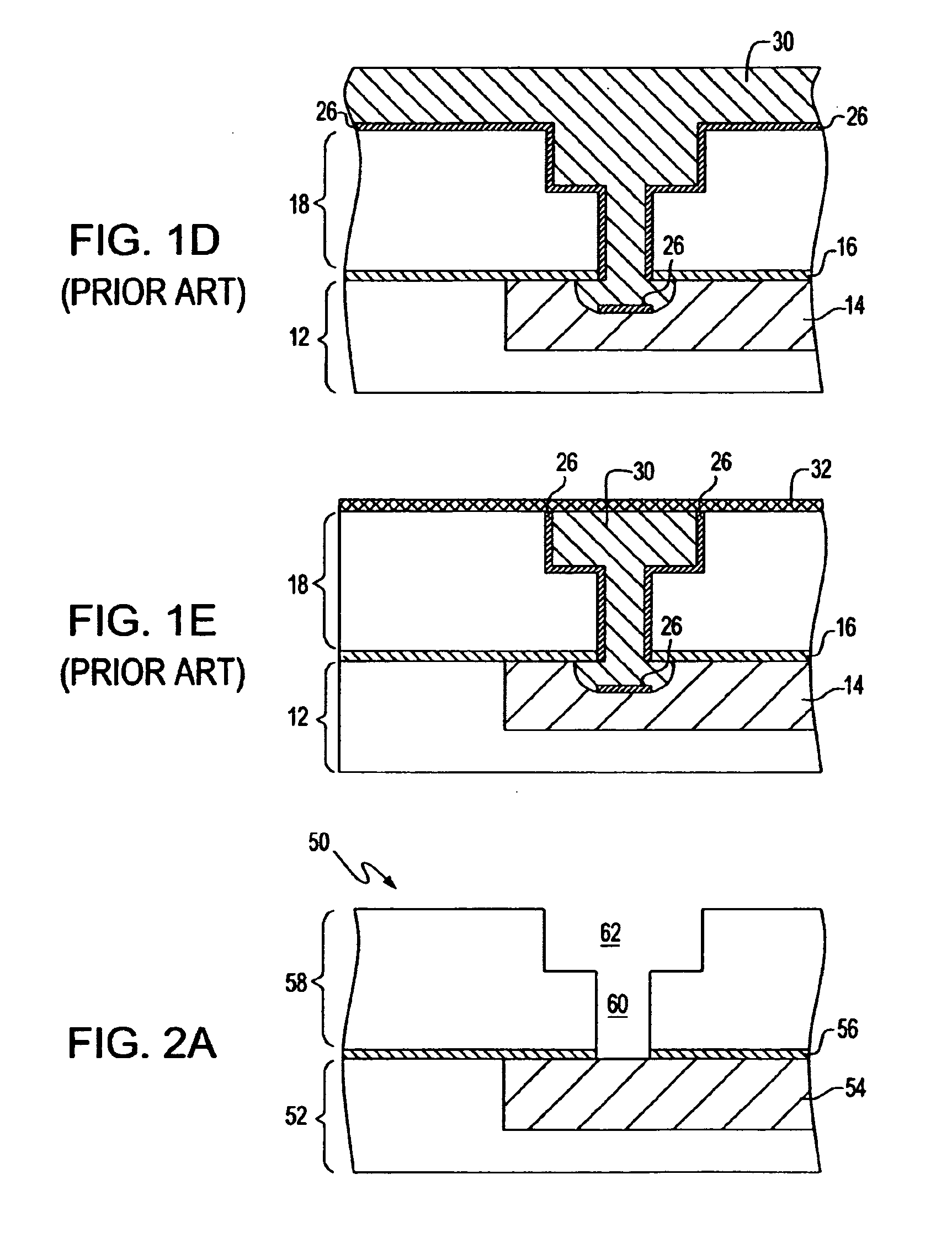
[0060] the present invention is now described in greater detail by referring to FIGS. 2A-2E. FIG. 2A shows an initial structure 50 prior to construction of the anchoring recessed area that includes a lower interlevel dielectric (ILD) 52 having at least one metal line 54 embedded therein. The metal line 54 is typically separated from the ILD 52 by a diffusion barrier (not shown). The initial structure also includes a first dielectric cap 56 having an opening that exposes a surface of the at least one metal line 54 atop the lower ILD 52. An upper ILD 58 having at least one via opening 60 and, optionally, at least one line opening 62 is located on the first dielectric cap 56. As illustrated, the at least one via opening 60 is located beneath the at least one line opening 62 and the at least one via opening 60 is substantially aligned with the opening provided in the first dielectric cap 56.

[0061] The processing of the initial structure 50 shown in FIG. 2A includes any conventional dual...

second embodiment

[0090] In an analogous manner to the construction illustrated in FIGS. 2A-2E and alternate structure can be produced. In this second embodiment, the structure is built in the same manner as the embodiment described above up until the formation of the structure shown in FIG. 2C, the analog structure shown in FIG. 3A is a line of sight deposition structure.

[0091] After producing the structure shown in FIG. 3A, a method to redistribute part of the liner and / or seed is employed to spread the liner and / or seed beyond the line of sight aperture, then a conductive material 68 such as, for example, a conductive metal or metal alloy, is deposited within the anchoring recessed area 64, the via opening 60 and the line opening 62 as well as atop the liner 66 that lies on the horizontal surface of the upper ILD 58. Examples of conductive material 68 that can be used in the present invention include, but are not limited to: W, Al, Cu, Ag, Al—Cu and other like conductive materials. Preferably, the...

third embodiment

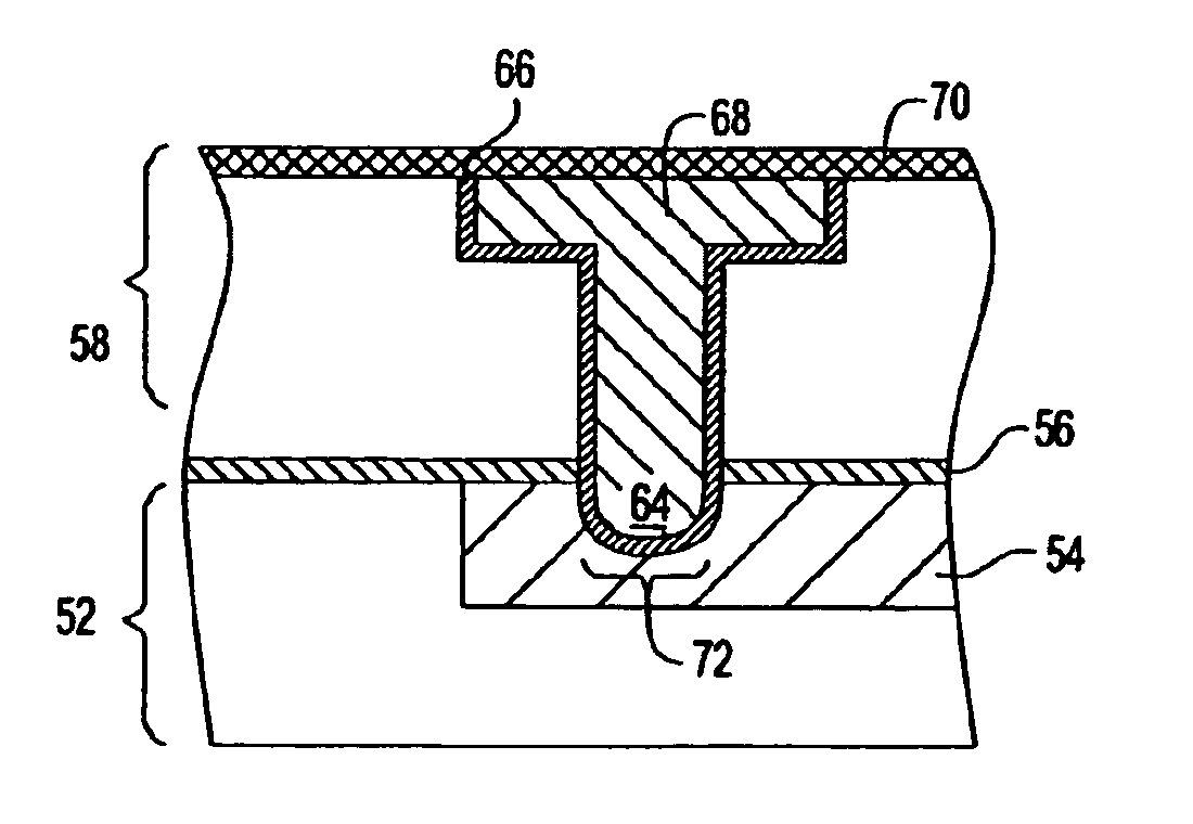
[0092]FIG. 4 shows another semiconductor Interconnect structure (e.g., third embodiment) that can be formed wherein the liner 66 is continuously present on the exposed surface of the etched metal line 54 within the anchoring recessed area 64, on the underside of the first dielectric cap 56 in the undercut provided during etching of the metal line 54, and on the exposed sidewalls of the upper ILD 58. In this embodiment of the present invention, the continuous liner 66 is formed by ALD or controlled resputtering during PVD deposition. All the other processing steps as described above are the same in forming the alternative structure shown in FIG. 4.

[0093] Reference will now be made to FIGS. 5A-5I which illustrate a fourth embodiment of the present invention. In the fourth embodiment of the present invention, a targeted oxidation process which enables a subsequent chemical etch process to selectively remove oxidized ILD and metal materials is employed. The resultant structure provides ...


PUM

PropertyMeasurementUnit
dielectric constantaaaaaaaaaa
resistanceaaaaaaaaaa

Abstract

Methods are provided that enable the ability to use a less aggressive liner processes, while producing structures known to give a desired high stress migration and electro-migration reliability. The present invention circumvents the issue of sputter damage of low k (on the order of 3.2 or less) dielectric by creating the via “anchors” (interlocked and interpenetrated vias) through chemical means. This allows the elimination or significant reduction of the sputter-etching process used to create the via penetration (“drilling, gouging”) into the line below in the barrier/seed metallization step. The present invention achieves the above, while maintaining a reliable copper fill and device structure.

Description

FIELD OF THE INVENTION [0001] The present invention relates to semiconductor integrated circuits, and more particularly to semiconductor interconnect structures including chemically formed anchored metallic vias. The present invention also provides methods of forming the inventive semiconductor interconnect structure. BACKGROUND OF THE INVENTION [0002] Generally, semiconductor devices include a plurality of circuits that form an integrated circuit including chips, thin film packages and printed circuit boards. Integrated circuits (ICs) can be useful for computers and electronic equipment and can contain millions of transistors and other circuit elements that are fabricated on a single silicon crystal substrate. For the device to be functional, a complex network of signal paths will normally be routed to connect the circuit elements distributed on the surface of the device. Efficient routing of these signals across the device can become more difficult as the complexity and number of ...

Claims


Application Information

Patent Timeline
Patent Type & Authority Applications(United States)
IPC IPC(8): H01L23/48H01L21/4763
CPCH01L21/76802H01L2924/0002H01L21/76814H01L21/76843H01L21/76844H01L23/5226H01L23/53223H01L23/53238H01L23/53252H01L23/53266H01L23/5329H01L23/53295H01L21/76805H01L2924/00
Inventor MEHTA, SANJAY C.EDELSTEIN, DANIEL C.FITZSIMMONS, JOHN A.GRUNOW, STEPHANNYE, HENRY A. III.RATH, DAVID L.
Owner GLOBALFOUNDRIES US INC
Why Eureka
Try Eureka