Pattern inspection and measurement apparatus

a technology of pattern inspection and measurement apparatus, which is applied in the direction of instrumentation, originals for photomechanical treatment, semiconductor/solid-state device testing/measurement, etc., can solve the problems of large deterioration of repeatability of measuring dimensions, low detection rate of secondary signals, and unsatisfactory sn ratio of sem images, etc., to achieve high repeatability and high precision

Inactive Publication Date: 2008-01-24
HITACHI HIGH-TECH CORP
View PDF52 Cites 17 Cited by
  • Summary
  • Abstract
  • Description
  • Claims
  • Application Information

AI Technical Summary

Benefits of technology

[0024]Therefore, sample inspection and measurement technique that enables measuring dimensions and a configuration and inspecting a defect at higher precision and higher repeatability, compared with the conventional type can be provided by applying the sca

Problems solved by technology

According to the above-mentioned method, as secondary signals emitted from inspected material by the irradiation of the electron beam are detected in a divergent state by the detector, a detection rate of the secondary signals is low and the SN ratio of the SEM image is unsatisfactory.
When loc

Method used


Image

  • Pattern inspection and measurement apparatus
  • Pattern inspection and measurement apparatus
  • Pattern inspection and measurement apparatus

Examples


first embodiment

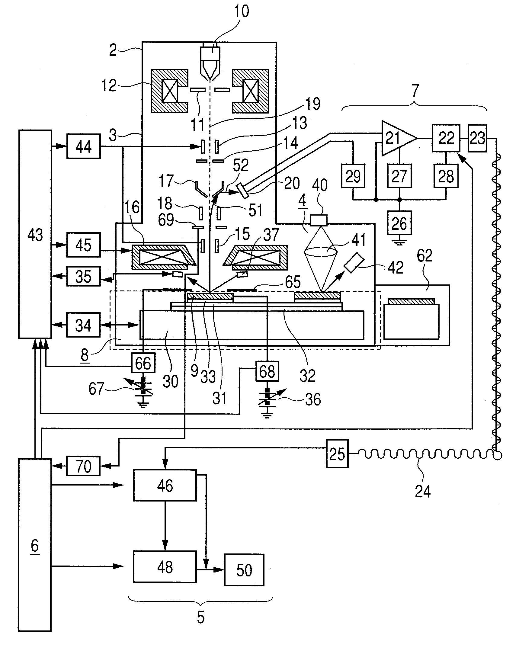
[0035]FIG. 1 shows the configuration of an inspection and measurement apparatus equivalent to a first embodiment. The inspection apparatus equivalent to this embodiment is a retardation type scanning electron microscope provided with a sample surface electrometer and an electrification control system and can be applied to inspection SEM, review SEM, measurement SEM and others.

[0036]The scanning electron microscope shown in FIG. 1s provided with an evacuated chamber 2 and a preliminary chamber (not shown in this embodiment) for carrying a wafer 9 as a sample into the chamber 2 and the preliminary chamber is configured so that it can be evacuated independently from the chamber 2. The inspection apparatus includes a controller 6 and an image processor 5 in addition to the chamber 2 and the preliminary chamber. The chamber 2 roughly includes an electro-optical system 3, the electrification control system, a detecting system 7, a sample housing 8 and an optical microscope 4. In this embo...

second embodiment

[0066]There is also a method of instructing a detector 20 to directly detect a secondary signal 51 accelerated from a wafer without using a reflector 17 and instructing a detecting system 7 to image. In this embodiment, the configuration of an apparatus and a setting method when the detector 20 is arranged outside an optical axis of a primary electron beam in such a method of directly detecting the secondary signal will be described. In this embodiment, the same reference numeral is allocated to a unit and others provided with the same function as those in the first embodiment and the description is omitted. In the configuration of the apparatus shown in FIG. 7, an image processor 5 and a controller 6 are included in the same information processor 100.

[0067]FIG. 7 shows the configuration of the inspection and measurement apparatus equivalent to a second embodiment. A secondary electron or a reflected electron or both 51 generated by radiating an electrode beam 19 onto a wafer 9 are ...

third embodiment

[0070]There is also a method of installing a detector 20 on a course (an optical axis) of a primary electron beam (a method of directly detecting a secondary signal). In this embodiment, the configuration of an apparatus and a setting method in that case will be described. In this embodiment, the same reference numeral is allocated to a unit and others provided with the same function as that in the first embodiment and the description is omitted.

[0071]FIG. 8 shows the configuration of an inspection and measurement apparatus equivalent to a third embodiment. A secondary electron or a reflected electron or both 51 generated by radiating an electron beam 19 onto a wafer 9 are accelerated by negative voltage applied to the wafer 9. A secondary signal converging lens 69 is arranged on the upside of the wafer 9 and hereby, the divergence of the secondary electrons or the reflected electrons or both 51 respectively accelerated is adjusted by the lens 69. A controller 70 that controls the l...


PUM


Abstract

Pattern inspection and measurement technique where the failure of the detection of a secondary signal due to the variation of an optical condition of a primary electron beam or the occurrence of an electric field perpendicular to a traveling direction of the primary electron beam in a surface of a wafer is minimized, an SEM image the SN ratio of which is high and which hardly has shading in a field of view can be acquired and measurement such as measuring the dimensions and configuration of a measured object and inspecting a defect is enabled at high precision and high repeatability. A lens for converging a secondary signal is installed in a position which a traveling direction of the primary electron beam crosses or on a course of the secondary signal spatially separated from the primary electron beam by Wien filter. An SEM image always free of shading caused by the failure of the detection of a secondary signal in the field of view can be acquired by providing a unit that changes the setting of the lens according to the optical condition such as retarding voltage and an electrification control electrode of the primary electron beam.

Description

CLAIM OF PRIORITY[0001]The present application claims priority from Japanese application JP 2006-199072 filed on Jul. 21, 2006, the content of which is hereby incorporated by reference into this application.FIELD OF THE INVENTION[0002]The present invention relates to the manufacturing technology of minute circuit patterns formed on a substrate for a semiconductor device and a liquid crystal display, particularly relates to the inspection and measurement technique of patterns for a semiconductor device and a photomask by an electron beam.BACKGROUND OF THE INVENTION[0003]Currently, in the manufacturing line of a semiconductor device, technique for inspecting and measuring a state of circuit patterns formed on a wafer on the way of a process fills an important role.[0004]This inspection and measurement technique has been mostly based upon an optical microscope, however, to cope with the recent miniaturization of a semiconductor device and the recent intricacy of a manufacturing process...

Claims


Application Information

Patent Timeline
IPC IPC(8): G01N23/00G01N23/225G03F1/84G03F1/86H01J37/10H01J37/244H01J37/28H01L21/027H01L21/66
CPCH01J37/244H01J37/266H01J37/28H01J2237/0492H01J2237/04924H01J2237/2817H01J2237/221H01J2237/24564H01J2237/24571H01J2237/2816H01J2237/21
Inventor CHENG, ZHAOHUIMAKINO, HIROSHITANIMOTO, KENJIOMORI, SEIKO
Owner HITACHI HIGH-TECH CORP
Why Eureka
Try Eureka