Flip-chip package substrate and a method for fabricating the same

a technology of flip-chip and package substrate, which is applied in the direction of printed circuit manufacturing, printed circuit aspects, non-metallic protective coating applications, etc., can solve the problems of low density of circuit layout, excessive layering, and inability to enhance the performance of electronic devices, so as to improve high-frequency operation, reduce the length and resistance of wires, and enhance circuit layout density

Active Publication Date: 2008-02-07
UNIMICRON TECH CORP
View PDF7 Cites 32 Cited by
  • Summary
  • Abstract
  • Description
  • Claims
  • Application Information

AI Technical Summary

Benefits of technology

[0008]In order to resolve the aforementioned disadvantages, the present invention provides a method for fabricating a flip-chip package substrate, comprising: providing a carrier plate; forming a patterned resistive layer having plural openings therein on the carrier plate; forming plural non-penetrating cavities corresponding to the openings on the surface of the carrier plate, and the carrier plate therefore has plural protrusions and a base; removing the patterned resistive layer; forming a circuit build-up structure on the surface of the carrier plate and, wherein the circuit build-up structure comprises at least a dielectric layer and at least a circuit layer; forming a resistive layer on the surface of the circuit build-up structure; removing the base of the carrier plate; removing the resistive layer to form an incomplete flip-chip package substrate for receiving a semiconductor chip; and respectively forming a solder mask on the upper and the lower surfaces of the flip-chip package substrate, and forming plural openings in the solder mask to expose part currents of the circuit build-up structure to function as conductive pads and the plural protrusions to function as conductive pads on the other surface of the circuit build-up structure. Thereby, the present invention provides a method for fabricating a flip-chip package substrate to enhance the density of circuit layout, reduce the length and the resistance of wires so as to improve the high-frequency operation. Moreover, the steps of the method are simple, and the stacks formed in this method are lessened so as to reduce the manufacturing cost of the flip-chip package substrate relative to prior art.

Problems solved by technology

Although more connecting ends are provided, the performance of electronic devices cannot be enhanced but is in fact restricted, owing to the over-long path of circuit and resulting high resistance for high frequency operation.
In the aforementioned method of providing a core-board, then accomplishing the inner structure by drilling, electroplating, plugging holes, forming the circuit and so on, and subsequently, realizing a multilayer package substrate by circuit build-up layer technology, some drawbacks exist such as low density of circuit layout, excessive layers, long circuit path, and high resistance.
Thereby, the electric property is poor in high frequency operation; in addition, the excessive layers result in the complex manufacturing processes and high manufacturing cost.

Method used


Image

  • Flip-chip package substrate and a method for fabricating the same
  • Flip-chip package substrate and a method for fabricating the same
  • Flip-chip package substrate and a method for fabricating the same

Examples


embodiment 1

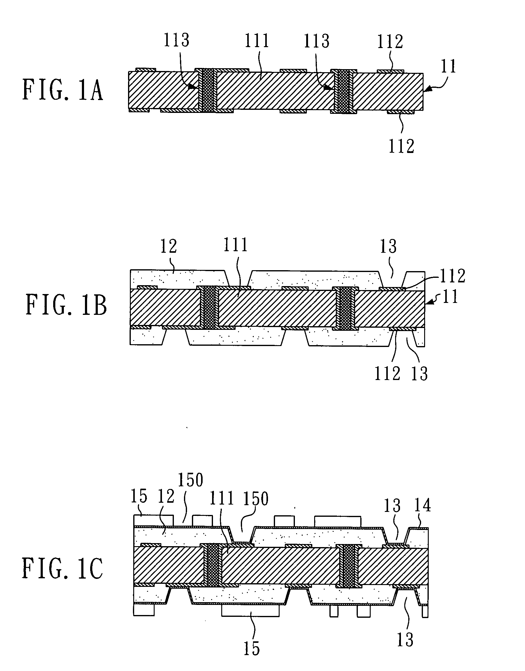
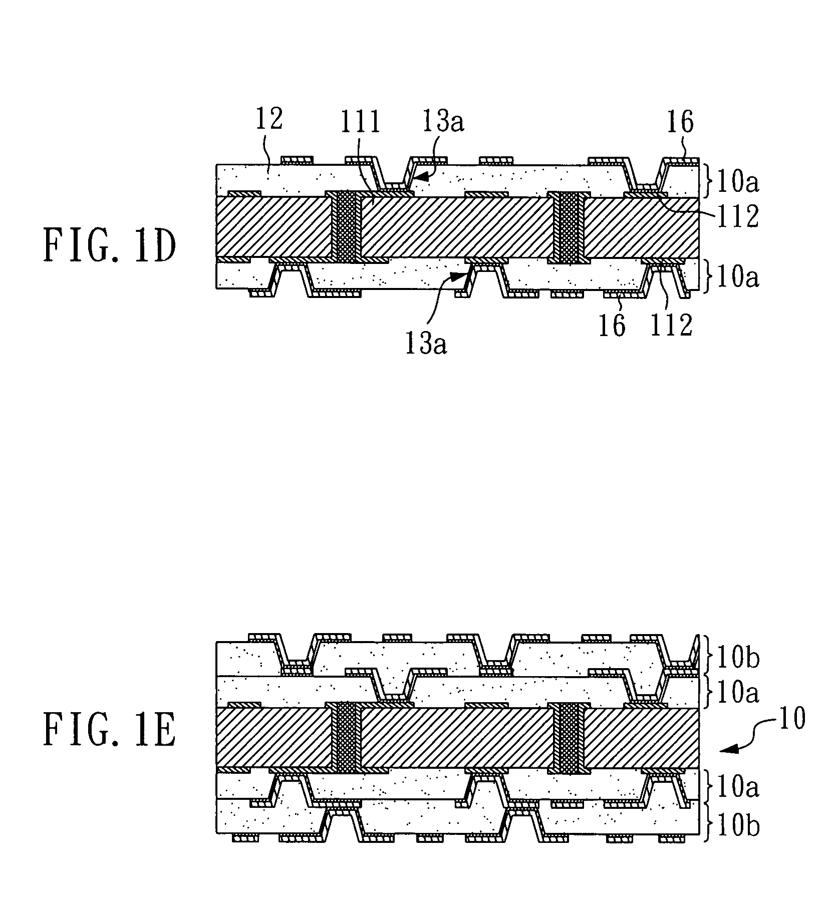
[0039]Please refer to FIGS. 2A to 2O, wherein cross-section views of a package substrate without a core-board of a preferred embodiment are shown. As shown in FIG. 2A, a metal carrier plate 201 is provided first. The material of the metal carrier plate 201 is metal, preferably, the material of the metal carrier plate 201 is copper. Subsequently, as shown in FIG. 2B, a resistive layer 202 such as a photosensitive resin layer is formed on the carrier plate and patterned to form plural openings 203 in the resistive layer 202 by exposure and development. Next, as shown in FIG. 2C, plural non-penetrating cavities 204 corresponding to the openings 203 are formed on the carrier plate 201, and thereby the carrier plate 201 has plural protrusions 201b and a base 201a. Then, as shown in FIG. 2D, the first patterned resistive layer 202 is removed.

[0040]Subsequently, as shown in FIG. 2E, a dielectric layer 205 is formed on the carrier plate and the non-penetrating cavities. The material of the ...

embodiment 2

[0046]Please refer to FIGS. 2A to 2M and 2N′ to 2O′, wherein cross-section views of a flip-chip package substrate structure of another embodiment are shown.

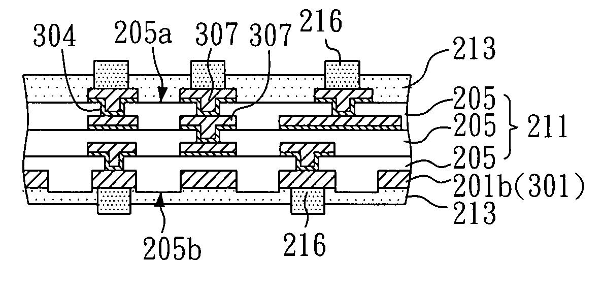
[0047]An incomplete flip-chip package substrate is provided by repeating the steps of FIGS. 2A to 2M first. Subsequently, as shown in FIG. 2N′, metal posts 218 and then solder bumps 216 are formed by electroplating. Preferably, the material of the metal posts 218 is selected from the group consisting of copper, nickel, chromium, titanium, a copper / chromium alloy, and a tin / lead alloy. More preferably, the material of the metal posts 218 is copper. Next, as shown in FIG. 2O′, retaining components 219 are respectively disposed around the peripherys of the solder mask 213 to inhibit the bend of the substrate.

[0048]Thereby, the present invention resolves the drawbacks of the carrier plate with a core-board, such as low density of circuit layout, excessive layers, long wires, and high resistance. The present invention provides a struc...


PUM


Abstract

The present invention provides a flip-chip package substrate and a method for fabricating a flip-chip package substrate comprising a circuit build-up structure, which comprises at least a dielectric layer and at least a circuit layer, wherein each dielectric layer comprises a first surface and a second surface, plural vias are formed in the first surface, the circuit layer is formed on the first surface and in the vias to electrically connect to another circuit layer disposed under the dielectric layer; a metal layer embedded in the exposed second surface of the circuit build-up structure without protruding the exposed second surface and connected to the circuit layer; and two solder masks disposed on the exposed first surface and the exposed second surface of the circuit build-up structure, wherein the solder masks have plural openings to separately expose part of the circuit layer and the metal layer functioning as conductive pads.

Description

BACKGROUND OF THE INVENTION[0001]1. Field of the Invention[0002]The present invention relates to a flip-chip package substrate and a method for fabricating the same, more particularly, to a structure of a flip chip substrate without plating through holes having improved density of circuit layout and a manufacturing method of a flip-chip package substrate to simplify the process.[0003]2. Description of Related Art[0004]In the development of electronics, the design trend of electronic devices is towards to multifunction and high-performance. Thus, high-density integration and miniaturization are necessary for a semiconductor package structure. On the ground aforementioned, the doublelayer circuit boards providing active components, passive components, and circuit connection, are being replaced by the multilayer circuit boards. The area of circuit layout on the circuit board increases in a restricted space by interlayer connection when meeting the requirement of high-density integratio...

Claims


Application Information

Patent Timeline
Patent Type & Authority Applications(United States)
IPC IPC(8): H01L23/532H01L21/44
CPCH01L21/6835H01L23/49822H01L2924/0002H01L23/49827H01L2924/3011H05K3/007H05K3/107H05K3/108H05K3/243H05K3/28H05K3/4007H05K3/4644H05K2201/0367H05K2201/0376H05K2203/0152H05K2203/1572H01L2924/00
Inventor WANG, HSIEN-SHOU
Owner UNIMICRON TECH CORP
Why Eureka
Try Eureka