Semiconductor device and method of manufacturing the same

Active Publication Date: 2008-02-14
RENESAS ELECTRONICS CORP
View PDF8 Cites 19 Cited by
  • Summary
  • Abstract
  • Description
  • Claims
  • Application Information

AI Technical Summary

Benefits of technology

[0012]It is an object of the invention to provide a power MISFET and a manufacturing method that make it possible to achieve miniaturization of the device str

Problems solved by technology

However, the advancement in shrinkage of the device structure is regulated by photolithography technologies in many ways, and currently, it is difficult to achieve miniaturization of the device structure while preventing side effects.
For example, the techniques disclosed in Japanese Patent laid-open Nos. 2000-196075 and Japanese Patent Laid-open No. 2000-277531 require alignment tolerance between the gate electrode and the contact hole for connecting with the source region, and therefore, with these techniques, it is difficult to improve the cell density.
However, with the structure described in Japanese Patent Laid-open No. 2002-246596, there is a problem that it is impossible to form an insulating film with a stable film thickness over the gate electrode and gate withstand voltage defects become apparent.
In this case, there are a range of constraints on miniaturization of the de

Method used


Image

  • Semiconductor device and method of manufacturing the same
  • Semiconductor device and method of manufacturing the same
  • Semiconductor device and method of manufacturing the same

Examples


first preferred embodiment

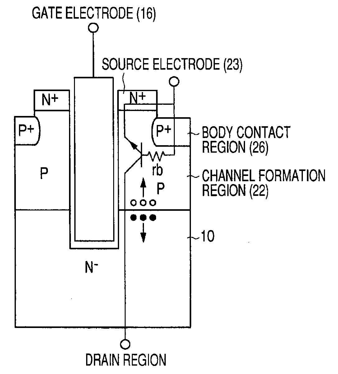
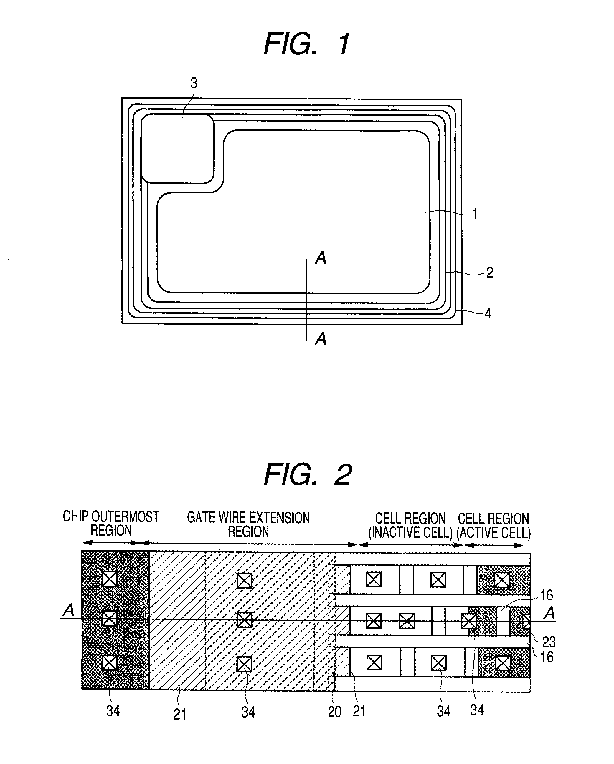
[0089]A semiconductor device according to a first preferred embodiment is described with reference to the drawings. FIG. 1 is a plan view illustrating an upper surface of the semiconductor chip over which a semiconductor device according to the first preferred embodiment is formed. As shown in FIG. 1, a source pad 1 made of, for example, an aluminum wire is formed in a central portion of the semiconductor chip. A gate wire 2 is formed so as to surround the source pad 1, and the gate wire 2 is coupled to a gate pad 3. A guard ring 4 is formed outward of the gate pad 3 and the gate wire 2 so as to surround the circumference of the semiconductor chip. The gate wire 2, the gate pad 3, and the guard ring 4 are also formed of, for example, aluminum wire. The guard ring 4 is a ring-shaped structure provided around the element formation region for the purpose of surface protection.

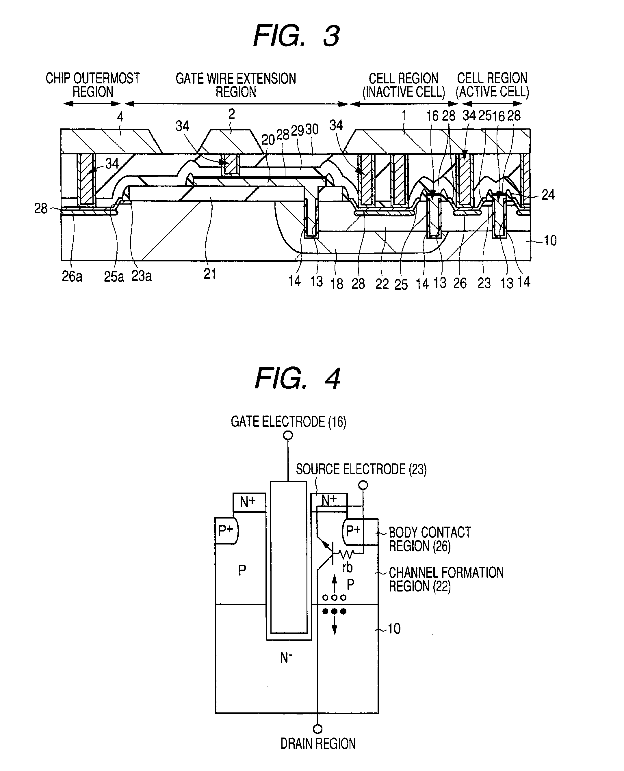
[0090]FIG. 2 is a schematic enlarged cross-sectional view taken along the line A-A in FIG. 1. FIG. 2 illustrate...

second preferred embodiment

[0145]A second preferred embodiment describes an example in which the source region is formed from a shallow source extension region and a deep source diffusion region. First, a manufacturing method of a power MISFET according to the second preferred embodiment is described with reference to the drawings.

[0146]The process steps from FIG. 5 through FIG. 15 are the same as described in the first preferred embodiment. Subsequently, as shown in FIG. 30, a source extension region 35 (first source region) the formation position of which is shallow is formed adjacent to a gate electrode 16 in the cell region (active cell) using a photolithography technique and an ion implantation technique. The source extension region 35 is a semiconductor region doped with an n-type impurity.

[0147]Next, as shown in FIG. 31, a silicon oxide film is formed over the entire surface of the main surface of the semiconductor substrate 10, and thereafter, the sidewall 24 is formed on the side wall portion of the ...

third preferred embodiment

[0160]A third preferred embodiment describes an example in which the invention is applied to a technique for forming a power MISFET and a Schottky barrier diode in the same semiconductor chip.

[0161]FIG. 40 is a circuit diagram of a common synchronous rectifier-type DC / DC converter that uses power MISFETs, and FIG. 41 is a timing chart of the main-switch power MISFET Q1 and the synchronous rectifying power MISFET Q2 shown in FIG. 40. In FIG. 40, Q1 represents a main-switch power MISFET, Q2 represents a synchronous rectifying power MISFET, BD1 and BD2 represent body diodes, and SBD represents a Schottky barrier diode. Also, L represents inductance and C represents a capacitor element. The body diode BD1 and the body diode BD2 are incorporated in the main-switch power MISFET Q1 and the synchronous rectifying power MISFET Q2, respectively, and they are coupled in parallel. The Schottky barrier diode SBD is coupled in parallel to the synchronous rectifying power MISFET Q2.

[0162]The main-...


PUM


Abstract

A gate trench 13 is formed in a semiconductor substrate 10. The gate trench 13 is provided with a gate electrode 16 formed over a gate insulating film 14. A portion of the gate electrode 16 protrudes from the semiconductor substrate 10, and a sidewall 24 is formed over a side wall portion of the protruding portion. A body trench 25 is formed in alignment with an adjacent gate electrode 16. A cobalt silicide film 28 is formed over a surface of the gate electrode 16 and over a surface of the body trench 25. A plug 34 is formed using an SAC technique.

Description

CROSS-REFERENCE TO RELATED APPLICATIONS[0001]The disclosure of Japanese Patent Application No. 2006-216659 filed on Aug. 9, 2006, including the specification, drawings, and abstract is incorporated herein by reference in its entirety.BACKGROUND OF THE INVENTION[0002]1. Field of the Invention[0003]The present invention relates to semiconductor devices and manufacturing technologies, and more particularly to techniques effective for a power MISFET (Metal Insulator Semiconductor Field Effect Transistor) having a trench gate structure and manufacturing the same.[0004]2. Description of Related Art[0005]Japanese Patent Laid-open Nos. 2000-196075 and 2000-277531 disclose techniques for preventing a source offset by protruding a trench gate electrode from the surface of a semiconductor substrate.[0006]Japanese Patent Laid-open No. 2002-246596 discloses a manufacturing method of a power MISFET in which the cell pitch is reduced by a self-aligned structure. Specifically, it discloses a techni...

Claims


Application Information

Patent Timeline
IPC IPC(8): H01L21/336H01L29/772
CPCH01L21/26586H01L29/8725H01L29/0615H01L29/086H01L29/1095H01L29/41741H01L29/41766H01L29/42368H01L29/456H01L29/4933H01L29/66719H01L29/66727H01L29/66734H01L29/7806H01L29/7811H01L29/7813H01L29/7827H01L27/0629H01L21/76897H01L2224/0603
Inventor MATSUURA, HITOSHINAKAZAWA, YOSHITOKACHI, TSUYOSHIYATSUDA, YUJI
Owner RENESAS ELECTRONICS CORP
Why Eureka
Try Eureka