Semiconductor Device and Manufacturing Method Thereof

a technology of semiconductor devices and manufacturing methods, applied in the direction of semiconductor devices, thermoelectric device junction materials, electrical apparatus, etc., can solve problems such as deterioration of insulating films, and achieve the effects of easy charge separation, reduced applied voltage, and easy charge separation

Inactive Publication Date: 2008-02-21
SEMICON ENERGY LAB CO LTD
View PDF28 Cites 23 Cited by
  • Summary
  • Abstract
  • Description
  • Claims
  • Application Information

AI Technical Summary

Benefits of technology

[0017] According to the invention, charge separation easily occurs in the layer in which an inorganic compound having a charge-transfer complex is mixed with an organic compound. Then, the mixed layer, an insulator, and a conductor can constitute a capacitor, and hysteresis due to a charge to be stored in the capacitor occurs. A new memory element, to which this characteristic is applied, can be formed.
[0018] In addition, applied voltage can be reduced by employing, as a floating gate, such a layer in which charge separation easily occurs. Consequently, when the organic semiconductor device of the invention is utilized as a memory or the like, power consumption of an electronic device mounted with the memory can be reduced.
[0019] Further, since a carrier is not injected into an insulating film in the invention, deterioration of the insulating film can be prevented.

Problems solved by technology

In addition, there is concern about deterioration of the insulating film by performing such carrier injection.

Method used


Image

  • Semiconductor Device and Manufacturing Method Thereof
  • Semiconductor Device and Manufacturing Method Thereof
  • Semiconductor Device and Manufacturing Method Thereof

Examples


embodiment mode 1

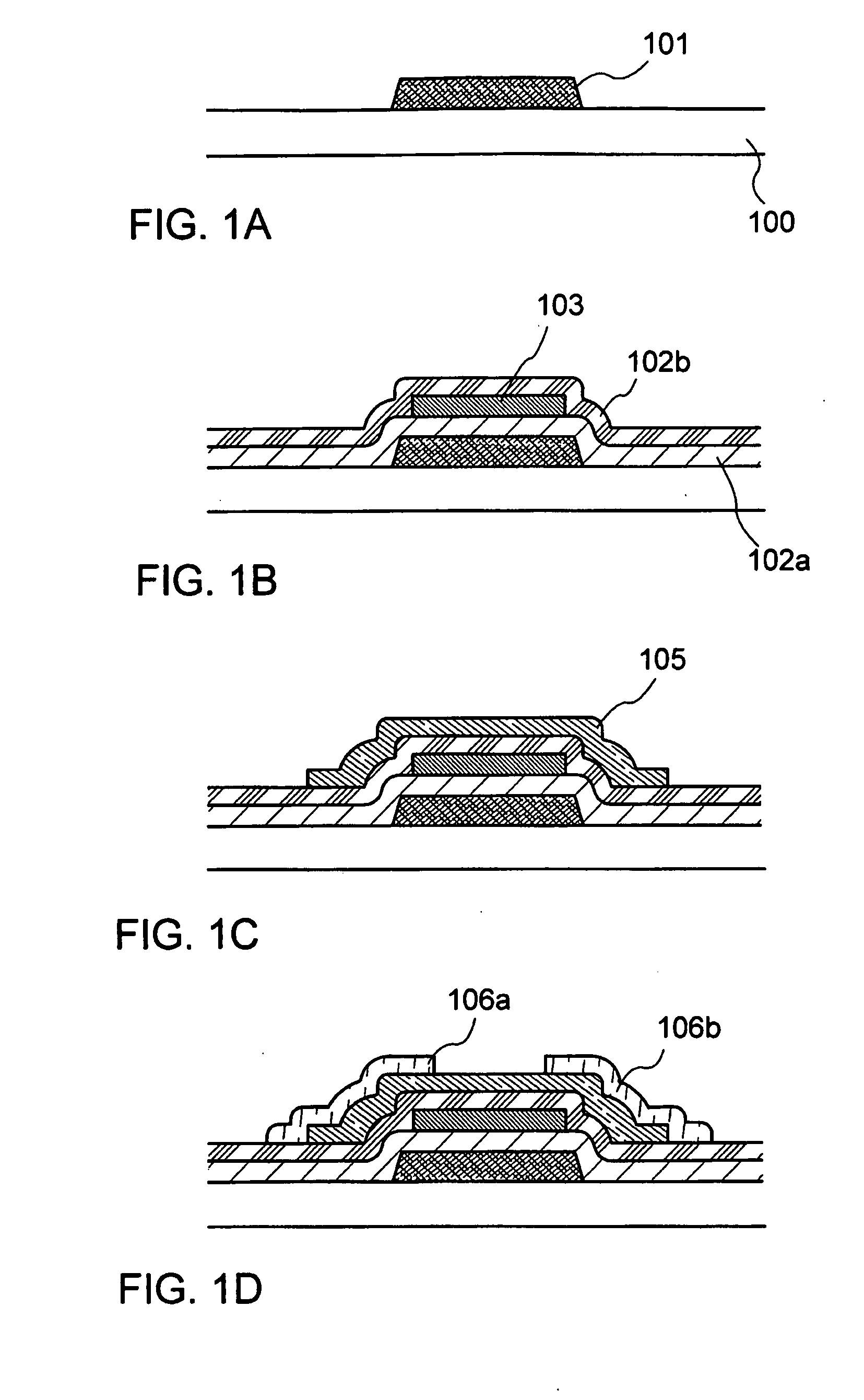
[0030] In this embodiment mode, explained is a method for manufacturing an organic semiconductor device, specifically an organic thin film transistor, having a layer in which an inorganic compound having a charge-transfer complex is mixed with an organic compound.

[0031] As shown in FIG. 1A, a substrate 100 having an insulating surface is prepared. For example, a glass substrate of barium borosilicate glass, alumino borosilicate glass, or the like, a quartz substrate, a stainless-steel (SUS) substrate, or the like can be used as the substrate 100. In addition, a substrate formed of a flexible synthetic resin such as plastic typified by PET (polyethylene terephthalate), PEN (polyethylerenaphthalate), or PES (polyethersulfone) or acrylic can be used since high-temperature treatment is not required in a manufacturing process of the organic semiconductor device of the invention.

[0032] A base film may be formed over the substrate 100. The base film is formed to prevent alkali metal or a...

embodiment mode 2

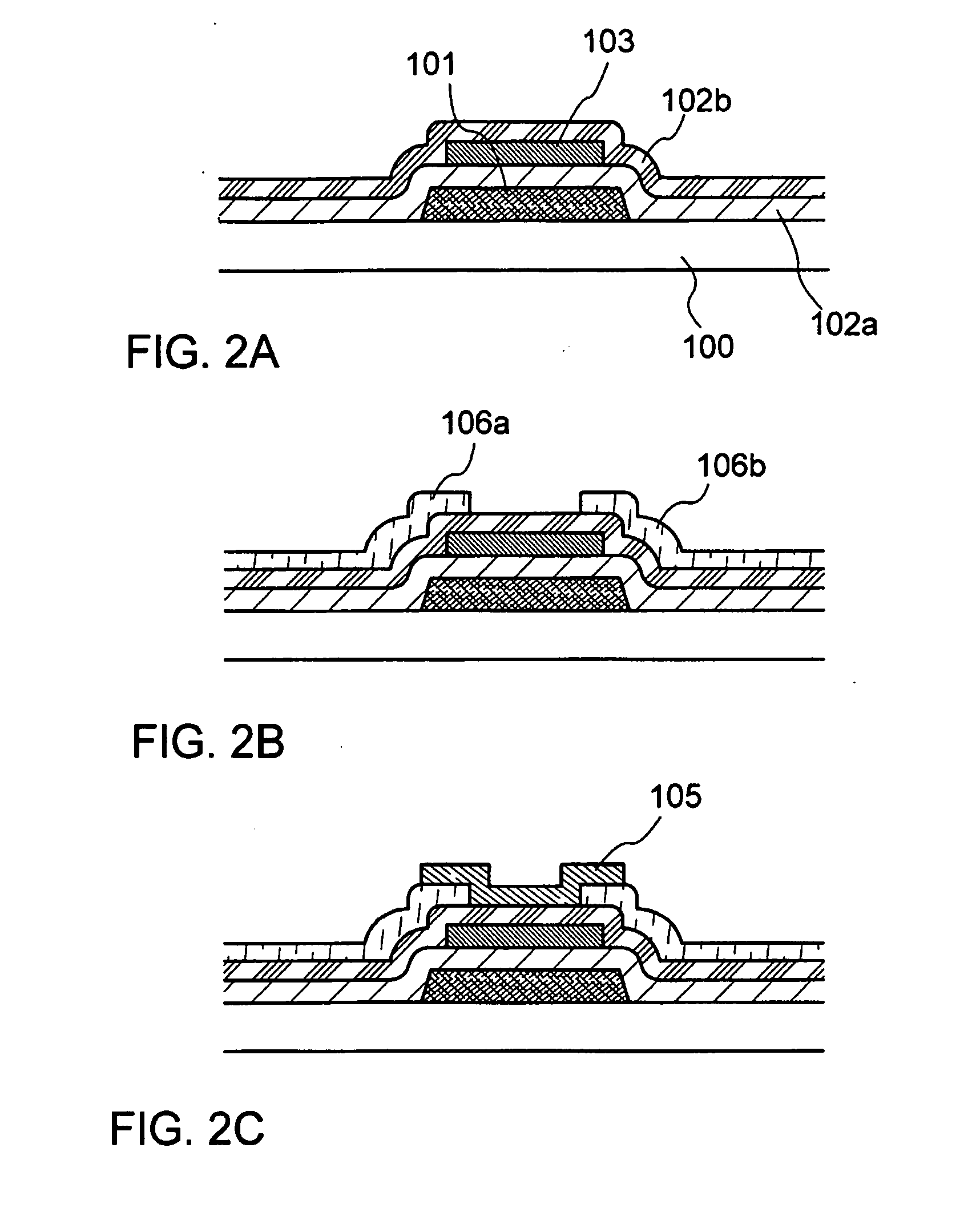
[0065] In this embodiment mode, explained is a structure of a so-called bottom contact type organic semiconductor device, which is different from the above embodiment mode.

[0066] As shown in FIG. 2A, a gate electrode 101 and a first insulating layer 102a which functions as a gate insulating film are formed over a substrate 100 similarly as in FIGS. 1A and 1B. A material, a manufacturing method, or the like of the substrate, the gate electrode, or the first insulating layer can be selected similarly as in the above embodiment mode.

[0067] Subsequently, a layer 103 in which an inorganic compound having a charge-transfer complex is mixed with an organic compound is formed. In this embodiment mode, the layer103 in which an inorganic compound having a charge-transfer complex is mixed with an organic compound is employed as a floating gate. Therefore, the layer 103 in which an inorganic compound having a charge-transfer complex is mixed with an organic compound is patterned so that a por...

embodiment mode 3

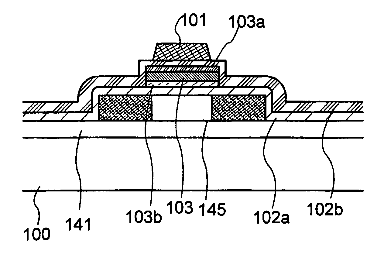
[0076] A structure of the invention, in which a layer where charge separation occurs is formed between insulating films and employed as a floating gate, can be employed in a semiconductor device including, as a semiconductor film, a film containing silicon that is an inorganic material. Thus, in this embodiment mode, explained is a semiconductor device, specifically a thin film transistor, in which a semiconductor film contains silicon, and which is different from the above embodiment mode.

[0077] As shown in FIG. 4, a silicon-containing semiconductor film 145 is formed over a substrate 100 with a base film 141 therebetween. As for the base film 141, an insulating film of silicon oxide, silicon nitride, silicon nitride oxide, or the like can be used as described in the above embodiment mode. In a semiconductor device described in this embodiment mode, the semiconductor film 145 is formed near the substrate 100. Thus, the base film 141 is preferably provided actively.

[0078] Subseque...


PUM


Abstract

A nonvolatile memory has a problem in that applied voltage is high. This is because a carrier needs to be injected into a floating gate through an insulating film by a tunneling effect. In addition, there is concern about deterioration of the insulating film by performing such carrier injection. An object of the present invention is to provide a memory in which applied voltage is lowered and deterioration of an insulating film is prevented. One feature is to use a layer in which an inorganic compound having a charge-transfer complex is mixed with an organic compound as a layer functioning as a floating gate of a memory. A specific example is an element having a transistor structure where a layer in which an inorganic compound having a charge-transfer complex is mixed with an organic compound and which is sandwiched between insulating layers is used as a floating gate.

Description

TECHNICAL FIELD [0001] The present invention relates to a semiconductor device having a memory function and a manufacturing method thereof. BACKGROUND ART [0002] A nonvolatile semiconductor memory having a floating gate can retain information even when power is turned off. Thus, it is mounted on many kinds of electronic devices. In such a nonvolatile semiconductor memory, it is important to control a thickness of an insulating film which covers the floating gate. For example, there is a method for forming a nonvolatile semiconductor memory by forming a capacitor insulating film and successively forming a conductive film (Reference 1: Japanese Patent Laid-Open No. 2004-140413). [0003] As a memory element, one having an organic semiconductor has been developed (Reference 2: Japanese Patent Laid-Open No. 2004-47791). Reference 2 discloses a switching memory element which includes an organic semiconductor memory layer exhibiting a hysteresis characteristic and a semiconductor diode laye...

Claims


Application Information

Patent Timeline
Patent Type & Authority Applications(United States)
IPC IPC(8): H01L51/10H01L51/40
CPCH01L21/28273H01L51/0059H01L51/0512H01L51/0078H01L51/0081H01L51/0062H01L29/40114H10K85/649H10K85/311H10K85/631H10K85/324H10K10/462H01L29/517
Inventor FURUKAWA, SHINOBUIMAHAYASHI, RYOTA
Owner SEMICON ENERGY LAB CO LTD
Why Eureka
Try Eureka