Organic Thin Film Transistor and Its Fabrication Method

a thin film transistor and fabrication method technology, applied in the direction of solid-state devices, semiconductor devices, thermoelectric devices, etc., can solve the problems of peeling electrodes, small grain size of film comprising grains, and inability to form inferior crystallinity, etc., to achieve improved carrier transportation efficiency, high device properties, and high grain size

Inactive Publication Date: 2008-02-21
SHARP KK
View PDF1 Cites 21 Cited by
  • Summary
  • Abstract
  • Description
  • Claims
  • Application Information

AI Technical Summary

Benefits of technology

[0032] An organic TFT of the invention comprises a film of an organic silane compound (an anchor film) between a gate insulating film and an organic thin film and carriers can be transported through both of the anchor film and the organic thin film, so that the carrier transportation efficiency is improved and high device properties can be obtained.
[0033] Further, crystal growth of the organic thin film can be controlled by optimizing the π electron conjugated system molecules in the main skeleton part of the anchor film. Therefore, since it is made possible to form an organic thin film with a high grain size, the crystallinity of the organic thin film can be improved.
[0034] Further, with respect to the TFT of the present invention, without being affected by the formation method of the organic thin film, the crystallinity of the organic thin film can be controlled by the interaction of the π elec

Problems solved by technology

A material such as pentacene is strongly affected by the inorganic oxide composing the gate insulating film and prevented from stacking, which is a particular property of an organic material, so that there occurs a problem that the crystallinity of the semiconductor layer in the vicinity of the gate insulating film interface, that is, an accumulation layer of the carrier decrease.
Therefore, many adsorption sites are formed and as a result, only a film comprising grains with small grain sizes and having inferior crystallinity can be formed.
However, when an actual organic TFT is fabricated, if an inorganic

Method used


Image

  • Organic Thin Film Transistor and Its Fabrication Method
  • Organic Thin Film Transistor and Its Fabrication Method
  • Organic Thin Film Transistor and Its Fabrication Method

Examples


example 1

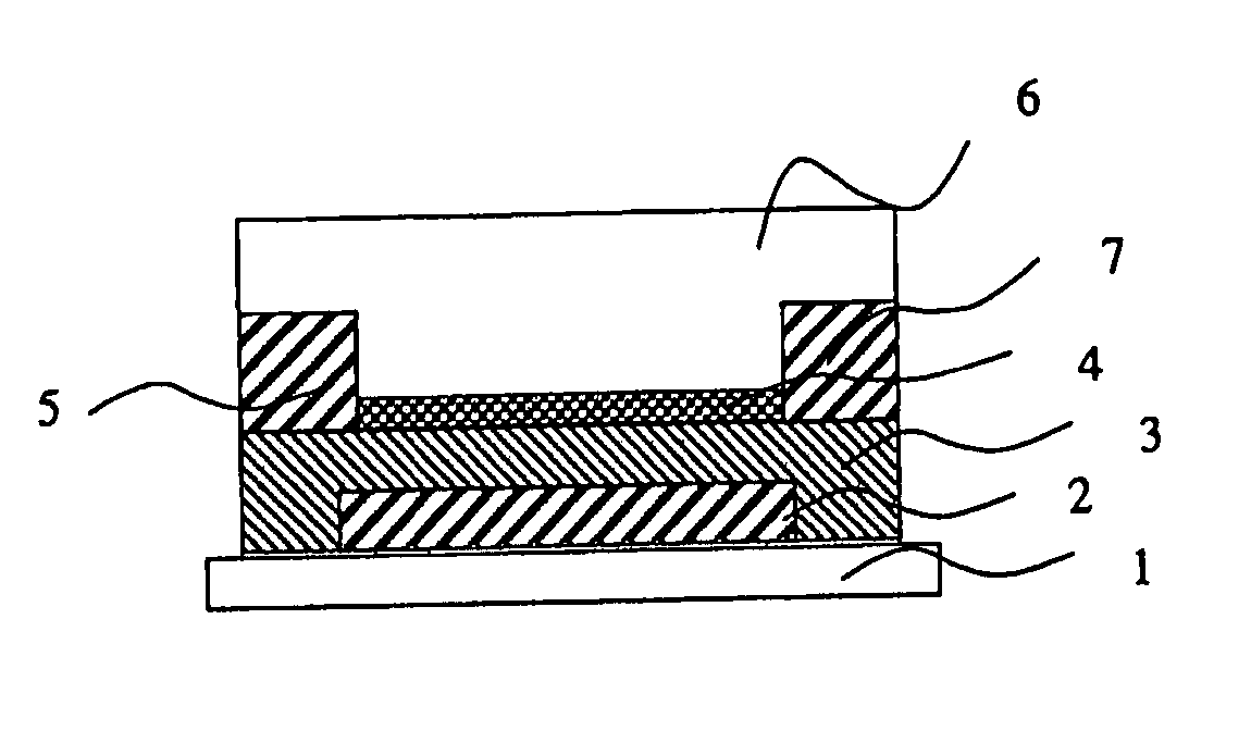
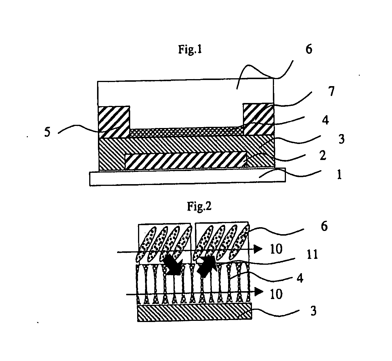
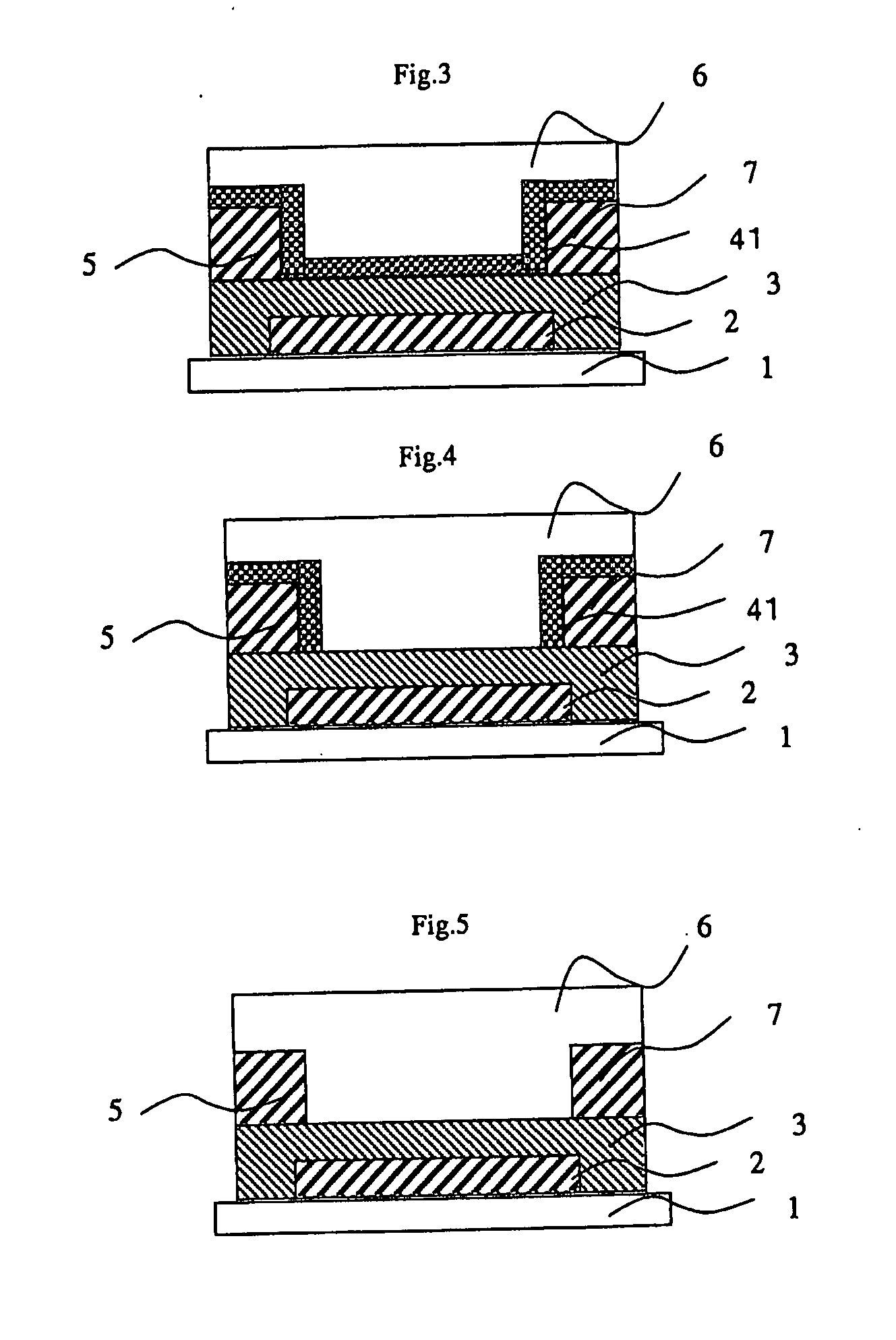
[0175] To fabricate an organic TFT shown in FIG. 1, chromium was first vapor-deposited on a substrate 1 of silicon to form a gate electrode 2.

[0176] Next, after a gate insulating film 3, which was a silicon nitride film, was deposited by a plasma CVD method, vapor-deposition of chromium and gold is carried out in this order and source / drain electrodes (5, 7) were formed by a conventional lithographic technique.

[0177] Successively, the obtained substrate was immersed in a mixed solution of hydrogen peroxide and concentrated sulfuric acid (mixing ratio 3:7) for 1 hour to make the surface of the gate insulating film 3 hydrophilic. After that, the obtained substrate was immersed in a 20 mM solution obtained by dissolving pentacene-triethoxysilane in a non-aqueous solvent (e.g. n-hexadecane) for 5 minutes in an aerobic condition, slowly pulled out of the solution, and washed with a solvent to form an anchor film 4. Successively, the resulting substrate was introduced into vacuum and a ...

example 19

[0196] First, a thin film of copper is formed on a silicon substrate by sputtering and successively, the obtained substrate was immersed in a mixed solution of hydrogen peroxide and concentrated sulfuric acid (mixing ratio 3:7) for 1 hour to carry out hydrophilicity improvement treatment. After that, the obtained substrate was immersed in a 20 mM solution obtained by dissolving naphthacene-triethoxysilane in a non-aqueous solvent (e.g. n-hexadecane) for 5 minutes in an aerobic condition, slowly pulled out of the solution, and washed with a solvent to form a buffer film. When the work function of the substrate obtained in the above-mentioned manner was measured by the Kelvin method, it was 5.1 eV.

examples 20 to 30

[0197] Substrate / copper / buffer film systems were obtained in the same manner as Example 19, except the raw materials for the buffer film were changed as shown in Table 6. The work function of each of the obtained systems was measured in the same manner as Example 19 and the results are shown in Table 6.

TABLE 6workfunctionEx.raw material of buffer film(eV)19naphthacene-triethoxysilane5.120anthracene-triethoxysilane5.721pentacene-triethoxysilane4.922hexacene-triethoxysilane4.623quaterthiophenetrichlorosilane6.124quinquethiophenetriethoxysilane5.5252-methylsexi-thiophenetrimethoxysilane5.0262-methylheptathiophene-trimethoxysilane4.8272-methyloctathiophene-trimethoxysilane4.628materials of Ex. 20 + Ex. 21 (1:1)5.029materials of Ex. 23 + 24 + 25 (1:1:1)5.530materials of Ex. 25 + 26 + 27 (1:1:1)4.8

[0198] The production methods of these raw materials of the buffer films in Table 6 will be described collectively as synthesis examples in the last part of Examples. In this connection, the r...


PUM

PropertyMeasurementUnit
Thicknessaaaaaaaaaa
Thicknessaaaaaaaaaa
Thicknessaaaaaaaaaa

Abstract

An organic TFT comprising an organic thin film, a gate electrode formed on one surface of the organic thin film through a gate insulating film, source/drain electrodes formed on both sides of the gate electrode and on one surface of the organic thin film or on the other surface, and a film of an organic silane compound positioned between the organic thin film and the gate insulating film and/or between the organic thin film and the source/drain electrodes.

Description

TECHNICAL FIELD [0001] The invention relates to an organic thin film transistor and its fabrication method. More particularly, the invention relates to an organic thin film transistor comprising a film of an organic silane compound and its fabrication method. BACKGROUND ART [0002] In recent years, IC technologies using transistors based on organic semiconductors have been proposed. Main advantageous points of the above-mentioned technologies are simplicity of fabrication methods and compatibility with flexible substrates. These advantages are expected to be employed in low-cost IC technologies suitable for applications such as smart cards, electronic tags, and displays. [0003] Today, as a film formation method to be employed at the time of fabricating a thin film transistor (TFT) using an organic semiconductor have been known a vacuum evaporation method and a coating method. These film formation methods make it possible to fabricate large scale devices with suppressed cost and to lo...

Claims


Application Information

Patent Timeline
IPC IPC(8): H01L51/10H01L51/40
CPCH01L51/0038H01L51/005H01L51/0052H01L51/0054H01L51/0055H01L51/0562H01L51/006H01L51/0068H01L51/0094H01L51/0533H01L51/0545H01L51/0058H10K85/114H10K85/60H10K85/623H10K85/615H10K85/622H10K85/655H10K85/626H10K85/633H10K10/476H10K85/40H10K10/486H10K10/466
Inventor NAKAGAWA, MASATOSHIHANATO, HIROYUKITAMURA, TOSHIHIRO
Owner SHARP KK
Why Eureka
Try Eureka