Method for Manufacturing Simox Substrate and Simox Substrate Obtained by the Method

a technology of simox substrate and simox substrate, which is applied in the direction of water-setting substance layered products, vacuum evaporation coatings, coatings, etc., can solve the problems of insufficient gettering effect and difficulty in forming oxygen precipitates, so as to reduce the concentration of heavy metal capturing in the defect collection layer, effectively capture heavy metal in the bulk layer, and reduce the effect of heavy metal capturing

Inactive Publication Date: 2008-02-21
SUMCO CORP
View PDF9 Cites 18 Cited by
  • Summary
  • Abstract
  • Description
  • Claims
  • Application Information

AI Technical Summary

Benefits of technology

[0030] A SIMOX substrate manufacturing method of the present invention makes it possible to efficiently capture heavy metal contamination due to subsequent ion implantation or high-temperature heat treatment into a bulk layer by oxygen precipitates formed through the second and third heat treatments by including a second heat treatment step and third heat treatment step before an oxygen ion implantation step or between the oxygen ion implantation step and the first heat treatment step or including a rapid heat treatment step, second heat treatment step, an

Problems solved by technology

Therefore, it has been said that it is difficult to form oxygen precipitates serving as internal gettering sink in a bulk layer through the high-temperature heat treatment.
Specifically, there are point defects in a single-crystal silicon wafer, that is, an interstitial point defect formed when Si atoms enter between lattices and a vacancy point defect privative in Si a

Method used


Image

  • Method for Manufacturing Simox Substrate and Simox Substrate Obtained by the Method
  • Method for Manufacturing Simox Substrate and Simox Substrate Obtained by the Method
  • Method for Manufacturing Simox Substrate and Simox Substrate Obtained by the Method

Examples


example 1

[0086] First, as shown in FIG. 3(a), there was prepared a CZ silicon wafer cut into a predetermined thickness from silicon ingot having oxygen concentration of 1.2×10¹⁸ atoms / cm3 (old ASTM) and a resistivity of 20 Ω·cm grown by the CZ method. Then, as shown in FIG. 3(b), rapid heat treatment was performed in which after continuously raising the temperature of the wafer under an ammonia gas atmosphere from 500 to 1,150° C. at 25° C. / second, the wafer was held at 1,150° C. for 15 seconds and then temperature is lowered up to 500° C. at the temperature lowering rate of 25° C. / second. Then, as shown in FIG. 3(c), second heat treatment for holding the rapid-heat-treated wafer 11 under a nitrogen atmosphere at 800° C. for 4 hours was applied to the rapid-heat-treated wafer 11. Then, as shown in FIG. 3(d), third heat treatment was performed which holds the rapid-heat-treated wafer 11 under a 3%-oxygen gas (nitrogen gas base) atmosphere at 1000° C. for 16 hours. Then, as shown in FIG. 3(e),...

example 2

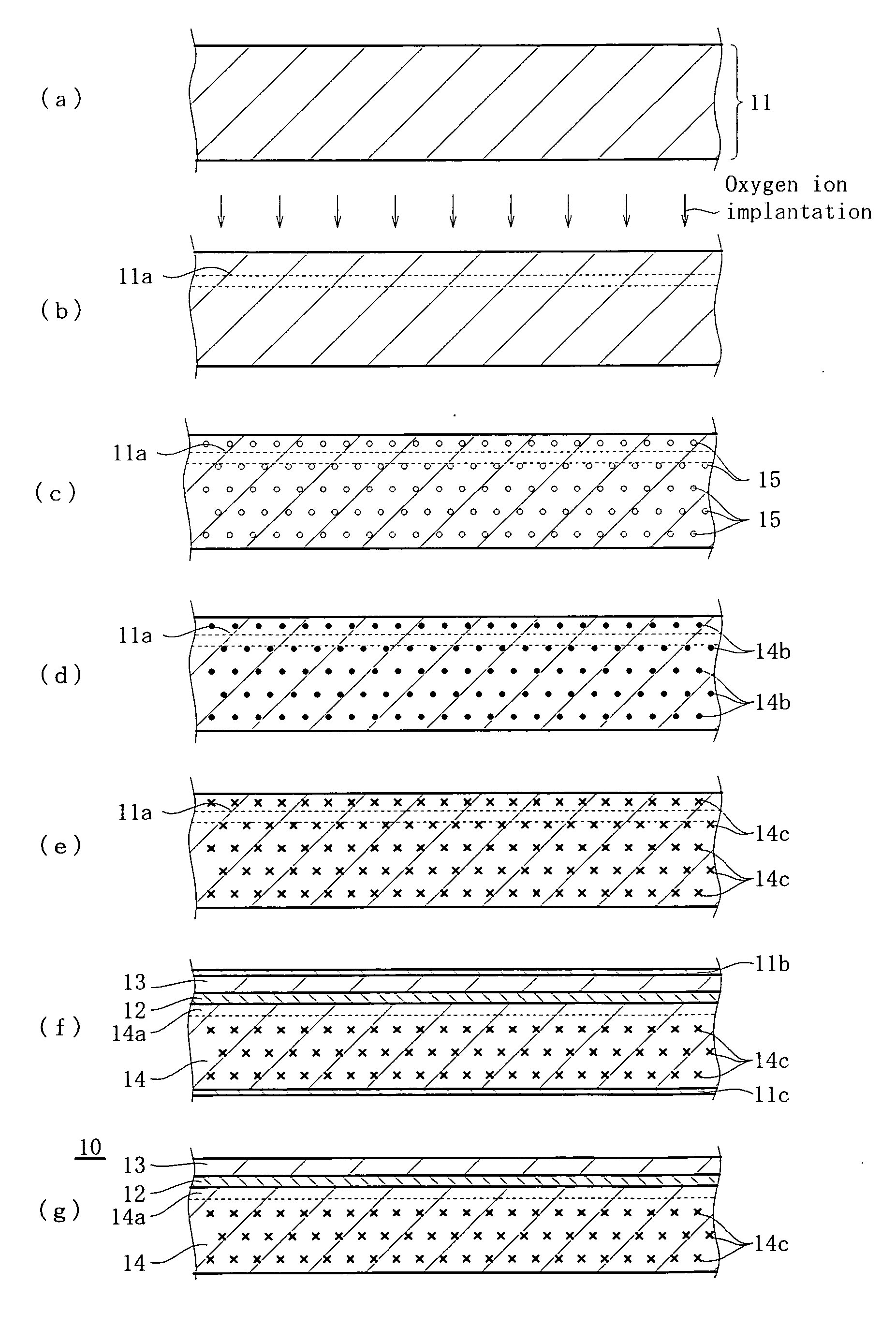
[0091] First, as shown in FIG. 4(a), there was prepared a CZ silicon wafer cut into a predetermined thickness from silicon ingot having an oxygen concentration of 1.2×10¹⁸ atoms / cm3 (old ASTM) and resistivity of 20 Ω·cm grown by the CZ method. Then, as shown in FIG. 4(b), the wafer is heated to a temperature of 550° C. or lower and in this state, oxygen ions were implanted into a predetermined region of the silicon wafer (for example, region at about 0.4 μm from the surface of a substrate) under the same conditions as in the above example 1. After implanting oxygen ions, SC-1 and SC-2 cleanings were applied to the surface of the wafer. Then, as shown in FIG. 4(c), the temperature of the wafer was continuously raised up to 500 to 1150° C. at 25° C. / second under an ammonia gas atmosphere and then the wafer was held at 1,150° C. for 15 seconds and then rapid heat treatment for lowering the temperature of the wafer up to 500° C. at temperature lowering rate of 25° C. / second was applied ...

example 3

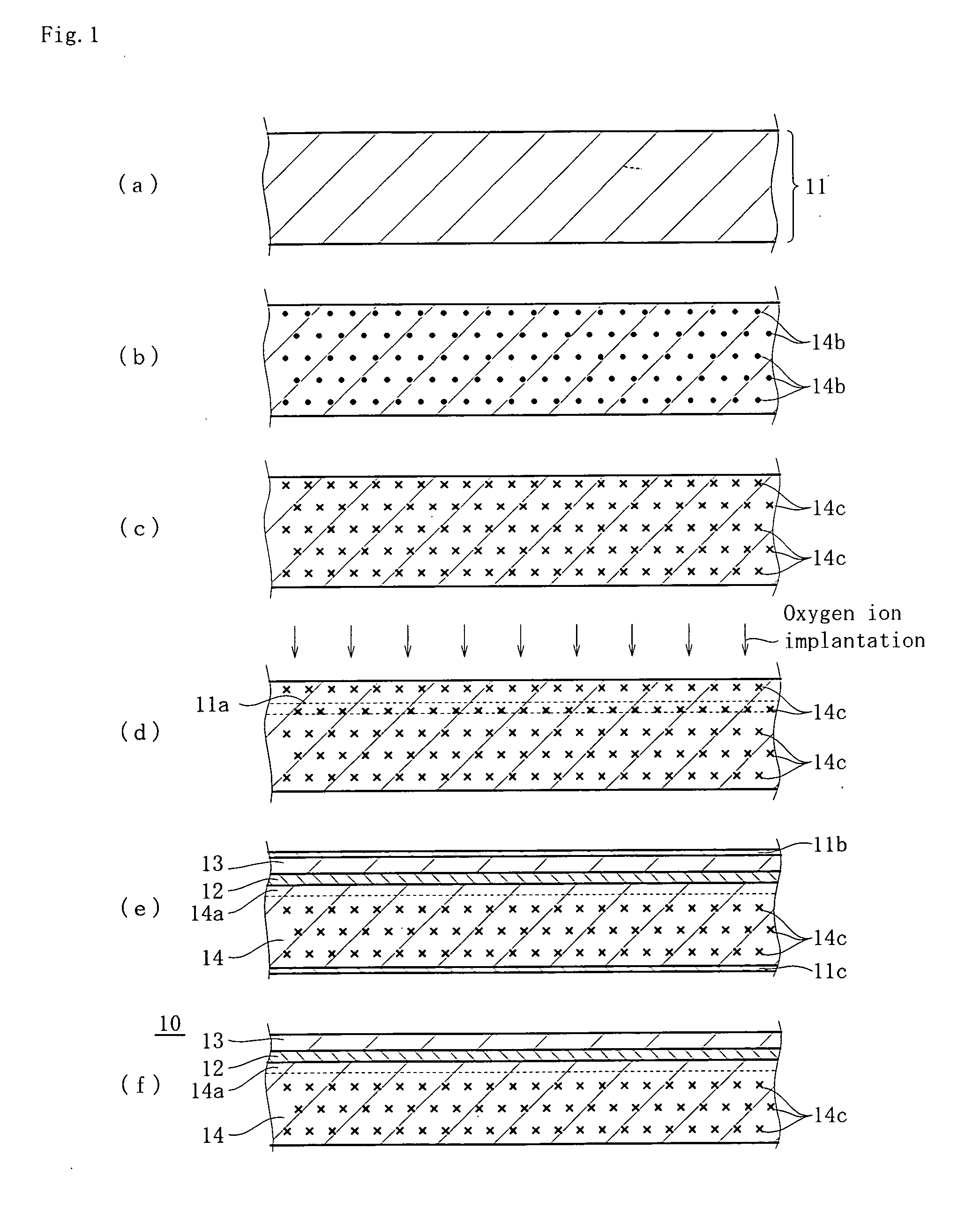
[0092] First, as shown in FIG. 1(a), there was a CZ silicon wafer cut into a predetermined thickness from silicon ingot having an oxygen concentration of 1.3×10¹⁸ atoms / cm3 (old ASTM), carbon concentration of 5×10¹⁶ atoms / cm3 (old ASTM) and a resistivity of 200 Ω·cm grown by the CZ method. Then, as shown in FIG. 1(b), second heat treatment was performed which held the wafer 11 under a 3%-oxygen gas atmosphere (argon gas base) at 800° C. for 4 hours. Then, as shown in FIG. 1(c), third heat treatment was performed which held the second-heat-treated wafer under a 3%-oxygen gas (argon gas base) atmosphere at 1000° C. for 8 hours. Then, as shown in FIG. 1(d), the wafer was heated to a temperature of 550° C. or lower and in this state, oxygen ions were implanted into a predetermined region of the silicon wafer (for example, region at about 0.4 μm from substrate surface) under the same conditions as in the above Example 1.

[0093] After implanting ions, SC-1 and SC-2 cleanings were applied ...


PUM

PropertyMeasurementUnit
Temperatureaaaaaaaaaa

Abstract

It is possible to efficiently capture heavy metal contamination due to ion implantation or high-temperature heat treatment in a bulk layer.
It is characterized that the present method comprises: a step of implanting oxygen ions into a wafer 11; a step of applying first heat treatment to a wafer under a predetermined gas atmosphere at 1,300 to 1,390° C. and forming a buried oxide layer 12 and an SOI layer 13 by applying first heat treatment to a wafer at 1,300 to 1390° C.; a second heat treatment step in which a wafer before oxygen ions are implanted has an oxygen concentration of 9×10¹⁷ to 1.8×10¹⁸ atoms/cm3 (old ASTM) and a buried oxide layer is formed entirely or locally in the wafer to form oxygen precipitate nuclei 14b formed in the wafer before the oxygen ion implantation step or between the oxygen ion implantation step and the first heat treatment step; and a third heat treatment step of growing oxygen precipitate nuclei 14b formed in the wafer so as to be oxygen precipitates 14c.

Description

TECHNICAL FIELD [0001] The present invention relates to a method for manufacturing a SIMOX and a SIMOX substrate obtained by the method among SOI (Silicon-On-Insulator) substrates in each of which a single-crystal silicon layer (hereafter referred to as SOI layer) is formed on a single crystal silicon body through a buried oxide layer according to the SIMOX (Separation by Implanted Oxygen) technique. More particularly, the present invention relates to a SIMOX substrate manufacturing method capable of efficiently capturing heavy metal contamination due to ion implantation or high-temperature heat treatment into the SIMOX substrate and a SIMOX substrate obtained by the method. BACKGROUND ART [0002] An SOI substrate (1) makes it possible to speed up a device operation because a parasitic capacitance between an element and a substrate can be decreased, (2) which is superior in radiation withstand voltage, and (3) which realizes high integration because dielectric separation is easy and ...

Claims


Application Information

Patent Timeline
IPC IPC(8): B32B9/00B32B7/00C23C14/48H01L21/322H01L21/02H01L21/762H01L27/12
CPCH01L21/76243H01L21/3225H01L27/12
Inventor ADACHI, NAOSHI
Owner SUMCO CORP
Why Eureka
Try Eureka