Surface Reconstruction Method for Silicon Carbide Substrate

Inactive Publication Date: 2008-02-28
SUMITOMO ELECTRIC IND LTD
View PDF4 Cites 12 Cited by
  • Summary
  • Abstract
  • Description
  • Claims
  • Application Information

AI Technical Summary

Benefits of technology

[0018] In accordance with the present invention, a surface reconstruction method for a silicon carbide substrate can be provided that can more simply close micropipes in a surface of the silicon carbide substrate.

Problems solved by technology

The silicon carbide substrate thus obtained using the modified Lely method, however, has a problem of generating many micropipes that have openings in a surface of the silicon carbide substrate and are hollow crystal defects extending in the direction of the c-axis.

Method used


Image

  • Surface Reconstruction Method for Silicon Carbide Substrate
  • Surface Reconstruction Method for Silicon Carbide Substrate
  • Surface Reconstruction Method for Silicon Carbide Substrate

Examples


example 1

[0033] First, a silicon carbide substrate made of a commercially available hexagonal silicon carbide crystal and in the shape of a disk with a diameter of two inches was prepared. For an off-plane inclined by 8° in the [11-20] direction with respect to the (0001) plane of the surface of the silicon carbide substrate, the micropipe density (number of micropipes / cm2) was checked by a method using-light scattering to find that the micropipe density was 96 (micropipes / cm2).

[0034] Next, on the off-plane of the silicon carbide substrate, a silicon film was formed by sputtering to a thickness of 100 nm. Then, in a heat-treatment furnace of an argon gas atmosphere at a pressure of 1×10⁵ Pa, the silicon carbide substrate and the silicon film were heat-treated at 1500° C.

[0035] Finally, the silicon film was removed by means of a liquid mixture of hydrofluoric acid and nitric acid. The micropipe density of the off-plane of the silicon carbide substrate from which the silicon film had been re...

example 2

[0037] First, as Example 1, a silicon carbide substrate made of a commercially available hexagonal silicon carbide crystal and in the shape of a disk with a diameter of two inches was prepared. For an off-plane inclined by 8° in the [11-20] direction with respect to the (0001) plane of the surface of the silicon carbide substrate, the mnicropipe density (number of micropipes / cm2) was checked by the same method as that of Example 1 to find that the micropipe density was 92 (micropipes / cm2).

[0038] Next, on the off-plane of the silicon carbide substrate, a silicon film was formed by sputtering to a thickness of 100 nm as Example 1. Then, in a heat-treatment furnace of an argon gas atmosphere at a pressure of 1×10⁵ Pa, the silicon carbide substrate and the silicon film were heat-treated at 1500° C.

[0039] Subsequently, in a heat-treatment furnace of an oxygen atmosphere at a pressure of 1×10⁵ Pa, the silicon carbide substrate and the silicon film were heat-treated at 1300° C. to produc...

example 3

[0040] First, as Example 1, a silicon carbide substrate made of a commercially available hexagonal silicon carbide crystal and in the shape of a disk with a diameter of two inches was prepared. For an off-plane inclined by 8° in the [11-20] direction with respect to the (0001) plane of the surface of the silicon carbide substrate, the micropipe density (number of micropipes / cm2) was checked by the same method as that of Example 1 to find that the micropipe density was 95 (micropipes / cm2).

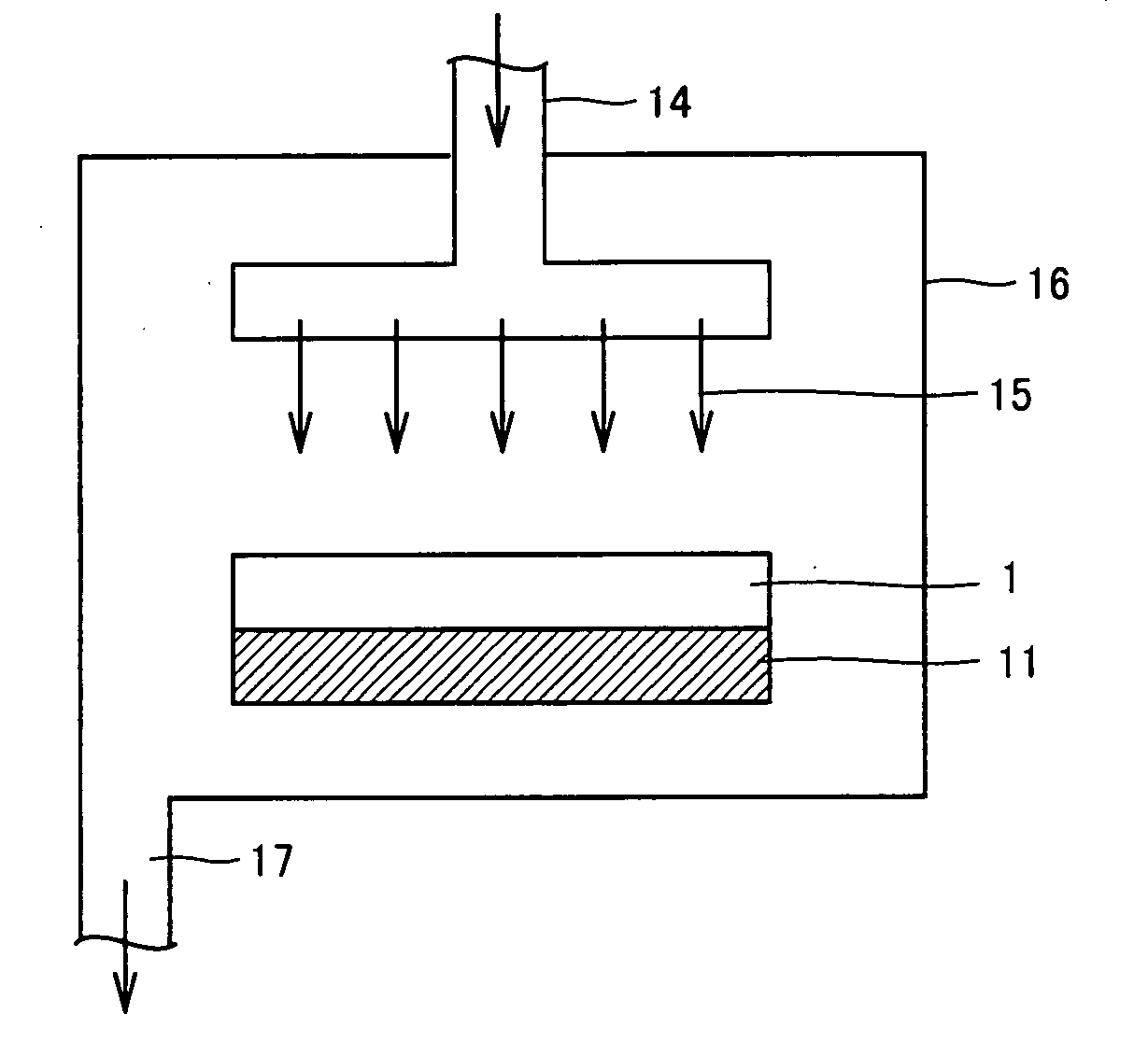
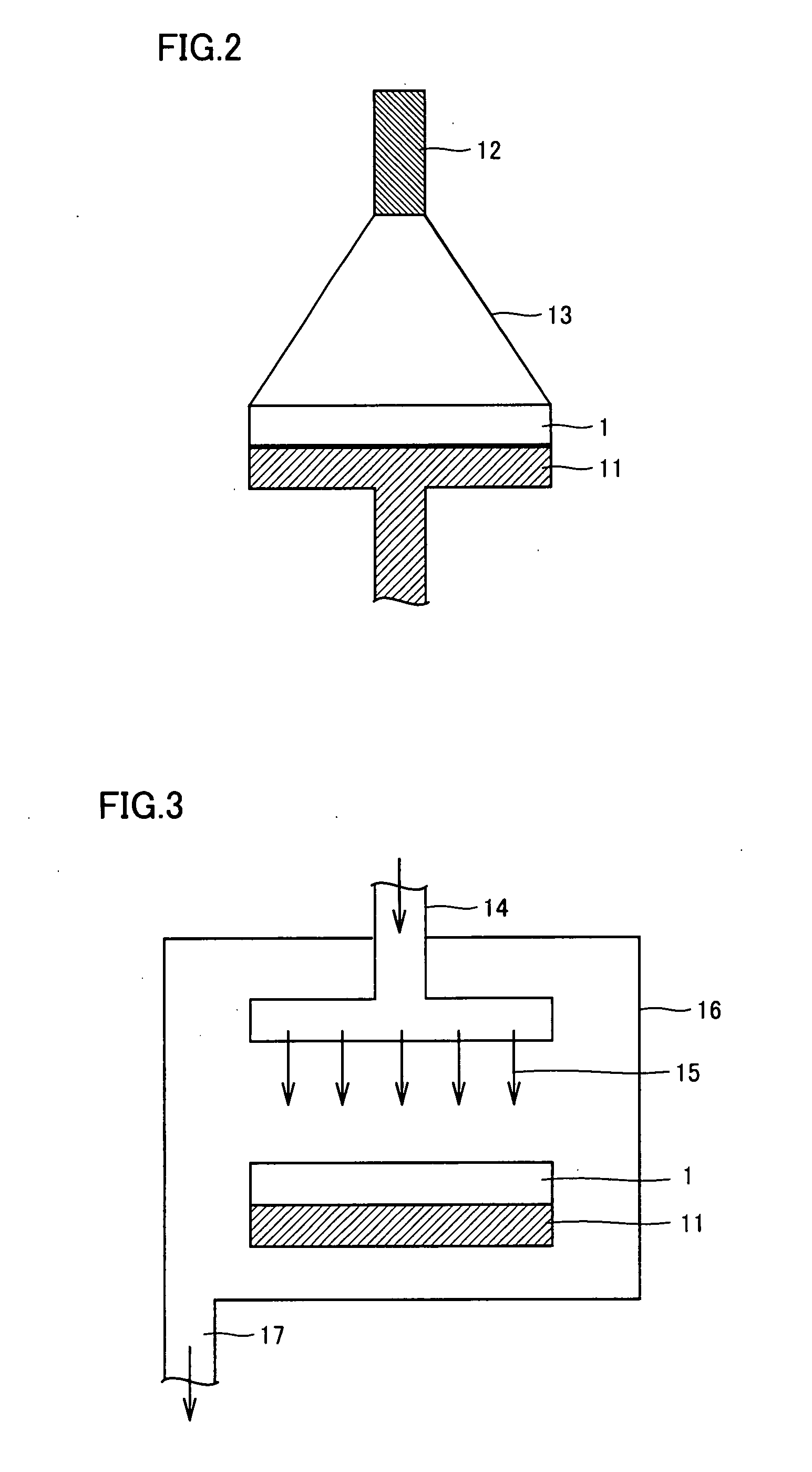
[0041] Next, as shown in the schematic cross section of FIG. 2, onto the off-plane of silicon carbide substrate 1 mounted on a substrate holder 11 and heated to 1500° C. in an argon gas atmosphere at a pressure of 1×10⁵ Pa, a liquid hexachlorodisilane (Si2Cl6) 13 as atomized was sprayed from a spray 12. Thus, on the off-plane of silicon carbide substrate 1, hexachlorodisilane 13 was thermally decomposed to form a silicon film on the off-plane of silicon carbide substrate 1 and, simultaneously, sili...


PUM

PropertyMeasurementUnit
thicknessaaaaaaaaaa
thicknessaaaaaaaaaa
thicknessaaaaaaaaaa

Abstract

A surface reconstruction method for a silicon carbide substrate (1) includes a silicon film forming step of forming a silicon film (2) on a surface of the silicon carbide substrate (1) and a heat treatment step of heat-treating the silicon carbide substrate (1) and the silicon film (2) without providing a polycrystalline silicon carbide substrate on a surface of the silicon film (2). Here, after the heat treatment step, a silicon film removal step of removing the silicon film (2) may be included. Further, a silicon oxide film forming step of oxidizing the silicon film (2) after the heat treatment step to generate a silicon oxide film, and a silicon oxide film removal step of removing the silicon oxide film may-be included.

Description

TECHNICAL FIELD [0001] The present invention relates to a surface reconstruction method for a silicon carbide substrate. In particular, the invention relates to a surface reconstruction method for a silicon carbide substrate that can more simply close micropipes in a surface of the silicon carbide substrate. BACKGROUND ART [0002] Silicon carbide (SiC) has a band gap approximately three times wider, a breakdown voltage approximately ten times higher, a saturated electron drift velocity approximately twice higher, and a thermal conductivity approximately three times higher, than those of silicon (Si), and thus silicon carbide has the characteristics that are not in silicon. Further, silicon carbide is a thermally and chemically stable semiconductor material. Therefore, it is expected that a device using a silicon carbide substrate is employed as a power device that surmounts physical limitations of a device using silicon or as an environment-resistant device operating at high temperat...

Claims


Application Information

Patent Timeline
Patent Type & Authority Applications(United States)
IPC IPC(8): H01L21/00
CPCC23C14/185C30B33/02C30B29/36C23C16/24C23C14/14
Inventor MASUDA, TAKEYOSHI
Owner SUMITOMO ELECTRIC IND LTD
Why Eureka
Try Eureka