Hotwall reactor and method for reducing particle formation in GaN MOCVD

a technology reactor, which is applied in the direction of chemically reactive gas growth, crystal growth process, polycrystalline material growth, etc., can solve the problems of gan film deposition process adding additional cost and time, hvpe also has drawbacks, and formation of anti-etch layer

Inactive Publication Date: 2008-02-28
APPLIED MATERIALS INC
View PDF13 Cites 60 Cited by
  • Summary
  • Abstract
  • Description
  • Claims
  • Application Information

AI Technical Summary

Benefits of technology

[0019]To address such needs and others, in certain aspects of the invention, a method of suppressing parasitic particle formation in a metal organic chemical vapor deposition process for deposition of III-V nitride films is provided. The method generally comprises: providing a substrate to a reaction chamber including at least a susceptor for supporting the substrate and a top-plate disposed above the substrate; introducing a Group-III organometallic precursor and at least nitrogen-containing precursor to the reaction chamber, wherein the nitrogen-containing precursor reacts with the Group-III organometallic precursor; and forming a deposition layer on the substrate from a reaction mixture comprising the Group-III organometallic precursor and the nitrogen-containing precursor under substantially isothermal reaction conditions such that parasitic particle formation is suppressed in the reaction chamber.

Problems solved by technology

However, the HVPE also has drawbacks for forming GaN and other III-V compound films.
At the very least, the formation of the anti-etch layer will add additional cost and time to the GaN film deposition process.
In addition, the high deposition rates that characterize HVPE processes make them difficult to use with low levels of dopant materials and for forming complex heterostructures.
Doping steps done after the GaN film is deposited may not provide an adequate concentration or homogeneity of the dopant in the film.
When post-deposition doping is possible at all, it will at the very least add additional cost and time to the GaN film deposition process.
Another major drawback of HVPE is the difficulty of using the process to grow alloys of III-V nitrides, such as aluminum gallium nitride (AlGaN) and indium gallium nitride (InGaN).
But unfortunately generating stable gas precursors for aluminum (e.g., aluminum chloride) and indium (e.g., indium chloride) has proven more difficult than the generation of GaCl.
MOCVD film depositions, however, also have drawbacks.
The slower deposition times make MOCVD a lower throughput and more expensive deposition process than HVPE.
Both approaches have had difficulties.
Scale up to large areas has proved difficult because the GaN must be grown at relatively high pressures (e.g., several hundred Torr), and at these pressures the flow velocity in a large reactor is low, unless the total flow through the reaction is made extraordinarily high.
Consequently, the precursor stream becomes depleted of reactants over a short distance, making it difficult to grow a uniform film over a large area.
Thus, there is competition between the desired film growth and the parasitic particle growth.
In the case of GaN films grown with a trimethylgallium precursor, the film growth rate eventually saturates with respect to the trimethylgallium flow, making it difficult to realize growth rates greater than about 5 μm / hr.
The formation of the parasitic particles can also degrade the optoelectronic qualities of the deposited GaN film.
However, attempts to dilute the precursor gas stream hurt the quality of the III-V film that was deposited.
Unfortunately, high total pressures and high ammonia flows are best for growing AlGaN films with these qualities, but growing these films with the requisite Al content by MOCVD is extremely challenging due to the formation of the parasitic particles.
While the formation of parasitic particles in MOCVD depositions of InGaN is not as pronounced as for AlGaN, it is still significant enough to limit the growth rate of the films.

Method used


Image

  • Hotwall reactor and method for reducing particle formation in GaN MOCVD
  • Hotwall reactor and method for reducing particle formation in GaN MOCVD
  • Hotwall reactor and method for reducing particle formation in GaN MOCVD

Examples


example 1

A. Example 1

Reduction in Particle Formation

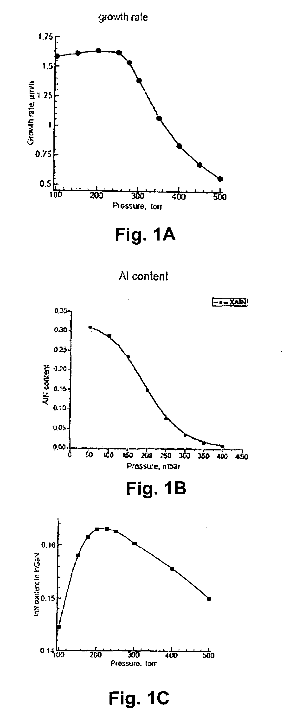
[0077]Simulations were run by STR of GaN film growth in a Thomas Swan reactor with a close-coupled showerhead injector within a hotwall reactor. Pressure was set to 200 Torr; reaction zone temperature was set to 1050° C.; inlet conditions were set to: NH3 15 slm, H2 20 slm, TMG 135 sccm; and bottom purge inlet was set to H2 3 slm. Results of the simulation showed approximately 13% Ga was in particle form at the outlet of the reaction, while approximately 2.6% of the Ga was in particle form at the back edge of the first wafer.

[0078]Additional simulations were run comparing varying plate temperatures, to demonstrate the effect on particulate distribution along the plate. Pressure was set to 200 Torr; reaction zone temperature was set to 1050° C.; inlet conditions were set to: NH3 15 slm, H2 20 slm, TMG 135 sccm; and bottom purge inlet conditions were set to: H2 3 slm. As shown in FIGS. 7A (1050° C. plate temperature), 7B (normal plate tempera...

example 2

B. Example 2

Increase in Deposition Rate Under Substantially Isothermal Conditions

[0079]Simulations were also run to investigate the effect of hotwall depositions on deposition rate. Pressure was set to 200 Torr; reaction zone temperature was set to 1050° C.; inlet conditions were set to: NH3 15 slm, H2 20 slm, TMG 27 sccm, and bottom purge inlet conditions were set to: H2 3 slm. As shown in FIG. 8, the top deposition rate was found for the 1050° C. plate (*), ranging from just above 12 μm / hr to just below 10 μm / hr. The radiatively heated plate (x) was found to have a deposition rate just above 10 μm / hr at the near end to just above 8 μm / hr at the far end, while the 30° C. plate (▴) was found to have a deposition rate of just above 8 μm / hr at the near end to just above 6 μm / hr at the far end. As such, the simulations predict improved deposition rates in hotwall reactors for reaction conditions as isothermal conditions are approximated.

[0080]The results of additional simulations are s...


PUM

PropertyMeasurementUnit
thicknessaaaaaaaaaa
pressureaaaaaaaaaa
temperatureaaaaaaaaaa

Abstract

Systems and methods to suppress the formation of parasitic particles during the deposition of a III-V nitride film with, e.g., metal-organic chemical vapor deposition (MOCVD) are described. In accordance with certain aspects of the invention, a hotwall reactor design and methods associated therewith, with wall temperatures similar to process temperatures, so as to create a substantially isothermal reaction chamber, may generally suppress parasitic particle formation and improve deposition performance.

Description

BACKGROUND OF THE INVENTION[0001]Group III-V semiconductors are increasingly being used in light-emitting diodes (LEDs) and laser diodes (LDs). Specific III-V semiconductors, such as gallium nitride (GaN), are emerging as important materials for the production of shorter wavelength LEDs and LDs, including blue and ultra-violet emitting optical and optoelectronic devices. Thus, there is increasing interest in the development of fabrication processes to make low-cost, high-quality III-V semiconductor films.[0002]One widely used process for making III-V nitride films like GaN is hydride vapor-phase epitaxy (HVPE). This process includes a high-temperature, vapor-phase reaction between gallium chloride (GaCl) and ammonia (NH3) at a substrate deposition surface. The GaCl precursor is produced by passing hydrogen chloride (HCl) gas over a heated, liquid gallium supply (melting point 29.8° C.). The ammonia may be supplied from a standard gas source. The precursors are brought together at th...

Claims


Application Information

Patent Timeline
Patent Type & Authority Applications(United States)
IPC IPC(8): H01L21/20
CPCC23C16/303C30B25/02C30B25/10C30B29/403C30B29/406H01L21/67109H01L21/0262H01L21/02378H01L21/02381H01L21/02403H01L21/0242H01L21/02458H01L21/0254H01L21/67115
Inventor BOUR, DAVIDSMITH, JACOBNIJHAWAN, SANDEEPWASHINGTON, LORI D.
Owner APPLIED MATERIALS INC
Why Eureka
Try Eureka