Variable period variable composition supperlattice and devices including same

a technology of variable period variable composition and supperlattice, which is applied in the direction of semiconductor devices, electrical devices, nanotechnology, etc., can solve the problems of significantly affecting optical output and device lifetime of devices, poor crystal quality of high aluminum-containing structural layers in typical deep uv light-emitting devices utilizing these templates, and inability to achieve high aluminum content heterostructure active regions, etc., to achieve the effect of facilitating the growth of high aluminum content active regions

Inactive Publication Date: 2008-03-06
PALO ALTO RES CENT INC
View PDF24 Cites 80 Cited by
  • Summary
  • Abstract
  • Description
  • Claims
  • Application Information

AI Technical Summary

Benefits of technology

[0012]The present invention is directed to facilitating the growth of high aluminum content heterostructure active regions on an initial AlGaN surface for UV light emitting devices such as light emitting diodes (LED) and laser diodes (LD). The initial AlGaN surface can, for example be an AlN or a GaN template on sapphire, an AlGaN template on silicon carbide, or a bulk AlN or GaN substrate. More specifically, the present invention is directed to systems and methods for providing an improved transition from an initial AlxGa1-xN surface (where 0≦x≦1) to a high-Al content MQWH active region. According to one em

Problems solved by technology

While significant improvements have been made in device reliability, optical power output, and mode stability, the performance of the nitride-based lasers and light emitting diodes emitting in the ultraviolet (UV) is still inferior to that of their blue or violet counterparts.
For example, differences in lattice constant between the substrate and the structural layers of the device significantly affects optical output and device lifetime.
The prior art AlGaN template layer formed over the typical Al2O3 substrate mitigates the problem somewhat, but the resulting crystal quality of the high aluminum-containing structural layers in typical deep UV light-emitting devices utilizing these templates are still very poor.
The high dislocation densities in typical AlGaN or AlN template layers on sapphire also pose significant problems for the light emitting device lifespan.
However, increasing the Al content

Method used


Image

  • Variable period variable composition supperlattice and devices including same
  • Variable period variable composition supperlattice and devices including same
  • Variable period variable composition supperlattice and devices including same

Examples


Embodiment Construction

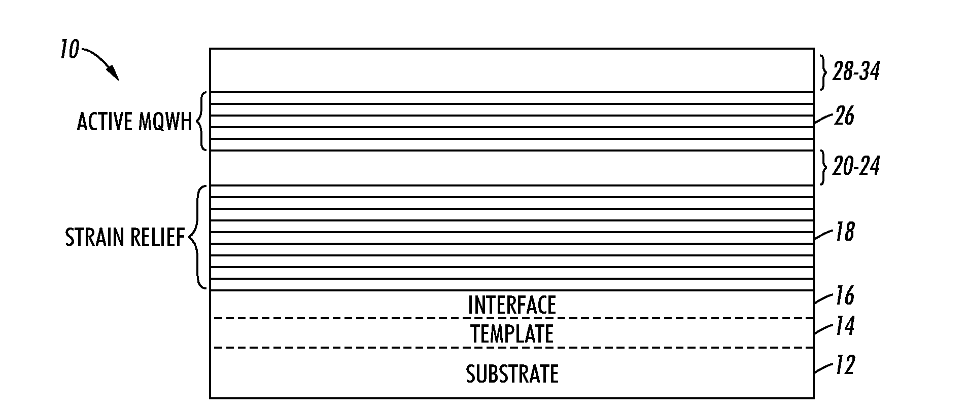
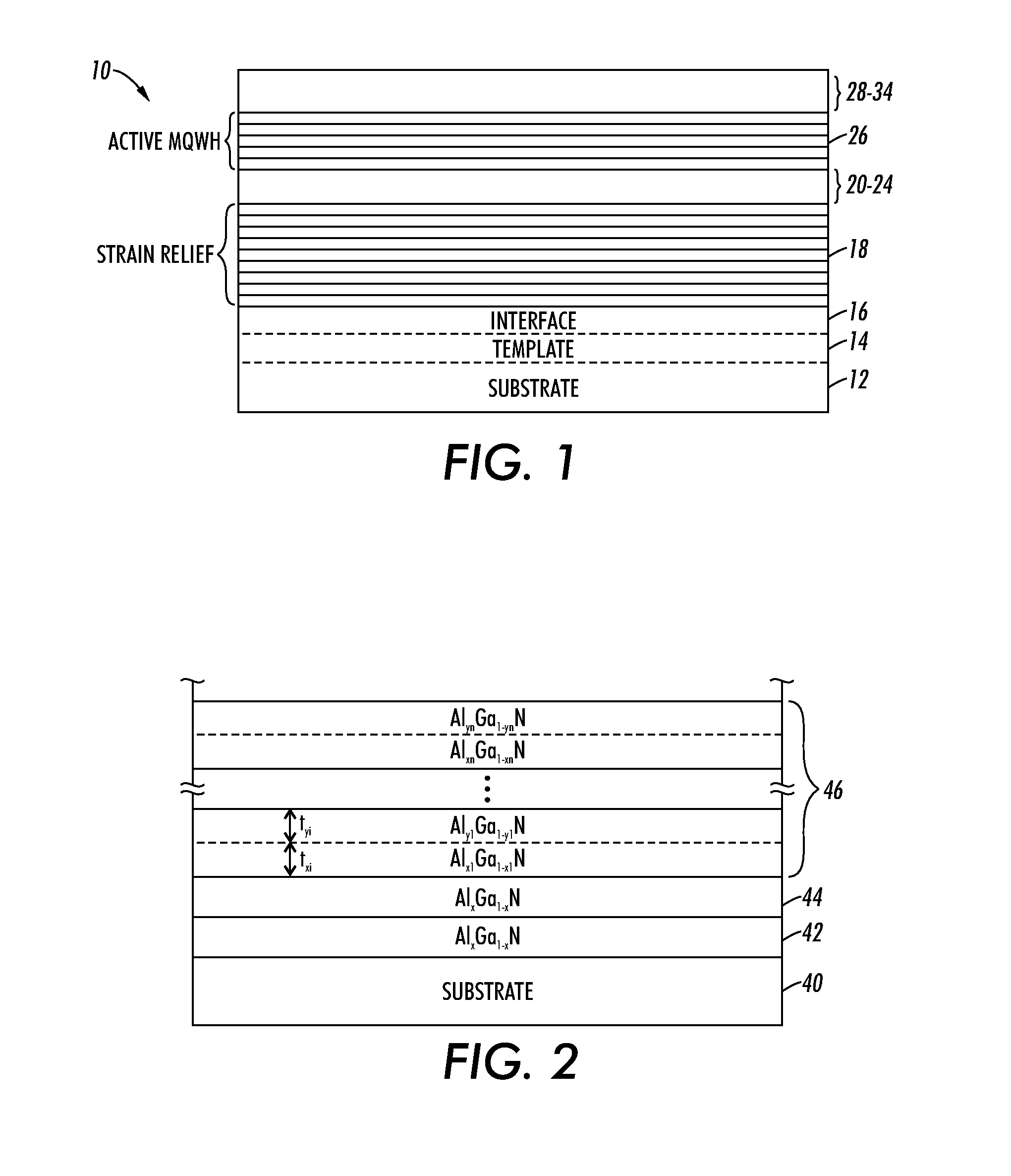
[0029]With reference now to FIG. 1, there is shown therein the general architecture of a heterostructure AlGaInN light emitting device structure 10 in accordance with the present invention. Diode structure 10 comprises a substrate 12. According to one embodiment of the present invention, substrate 12 may be Al2O3 (sapphire) on which is formed a template layer 14. As described further below, other substrates such as Silicon Carbide, bulk AlN, or bulk GaN may be employed. Template layer 14 may be AlN, but may also be AlxGa1-xN where x is not equal to 1. In some cases, template layer 14 is not necessary and is absent. Formed thereon is an optional interface layer 16. In the embodiment in which template layer 14 is AlN, interface layer 16, if present, is preferably also AlN.

[0030]Formed above interface layer 16 is variable period variable composition superlattice strain relief region 18 comprising a number of layer pairs, such as AlN / GaN, described further below. Additional layers, such...


PUM


Abstract

An optical semiconductor device such as a light emitting diode is formed on a transparent substrate having formed thereon a template layer, such as AlN, which is transparent to the wavelength of emission of the optical device. A variable period variable composition superlattice strain relief region is provided over the template layer such that the composition of the strain relief region approaches or matches the composition of the regions contiguous thereto. For example, the Al content of the strain relief region may be tailored to provide a stepped or gradual Aluminum content from template to active layer. Strain-induced cracking and defect density are reduced or eliminated.

Description

STATEMENT REGARDING FEDERALLY SPONSORED RESEARCH AND DEVELOPMENT[0001]The U.S. Government has a fully paid-up license in this invention and the right in limited circumstances to require the patent owner(s) to license others on reasonable terms as provided for by the terms of contract number N66001-02-C-8017 awarded by the Defense Advanced Research Projects Agency, and contract number DAAH01-03-9-R003 sponsored by the U.S. Army Aviation and Missile Command.BACKGROUND OF THE INVENTION[0002]1. Field of the Invention[0003]The present invention is related generally to the field of semiconductor light emitting devices, and more specifically to an architecture for an improved high-Al content, low defect quantum well light emitting device formed directly on a final substrate.[0004]2. Description of the Prior Art[0005]In the III-V compound semiconductor family, the nitrides have been used to fabricate visible wavelength light emitting device active regions. They also exhibit a sufficiently h...

Claims


Application Information

Patent Timeline
IPC IPC(8): H01L31/00H01L33/00H01L33/04
CPCB82Y20/00H01L21/0237H01L21/0242H01L21/02458H01L33/12H01L21/02507H01L21/0254H01L33/007H01L33/04H01L21/02505
Inventor CHUA, CHRISTOPHER L.YANG, ZHIHONGJOHNSON, NOBLE
Owner PALO ALTO RES CENT INC
Why Eureka
Try Eureka