

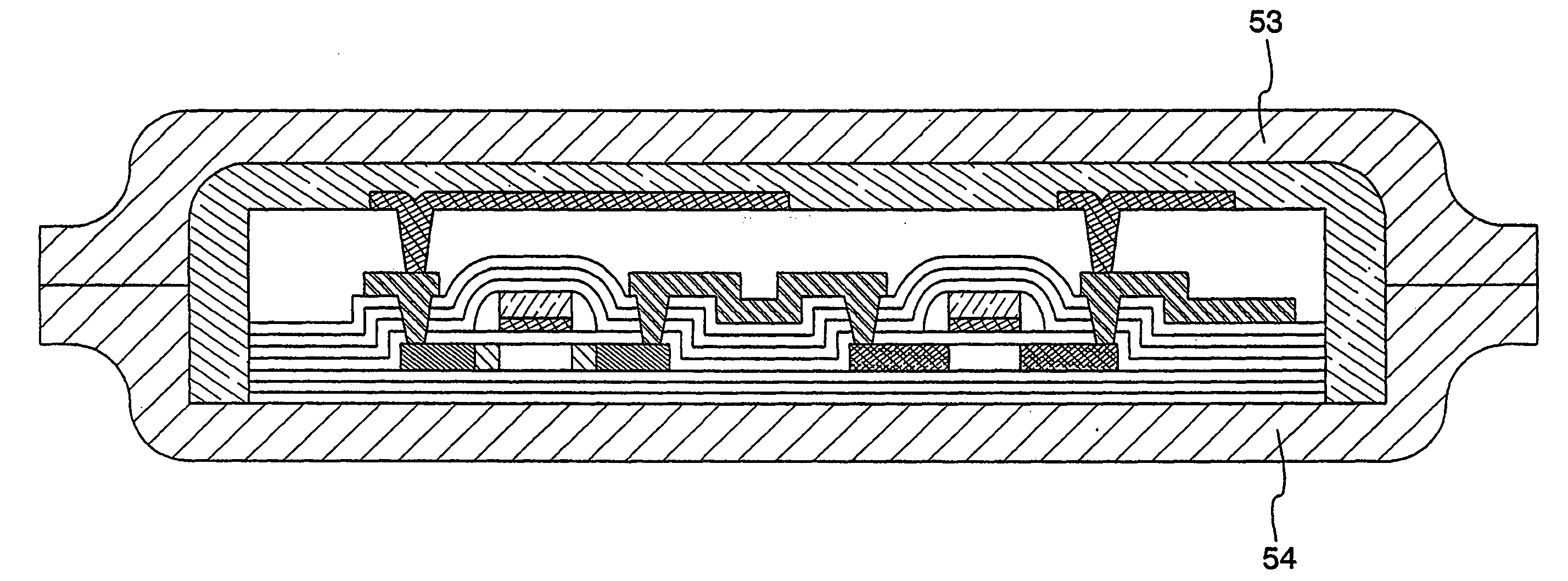
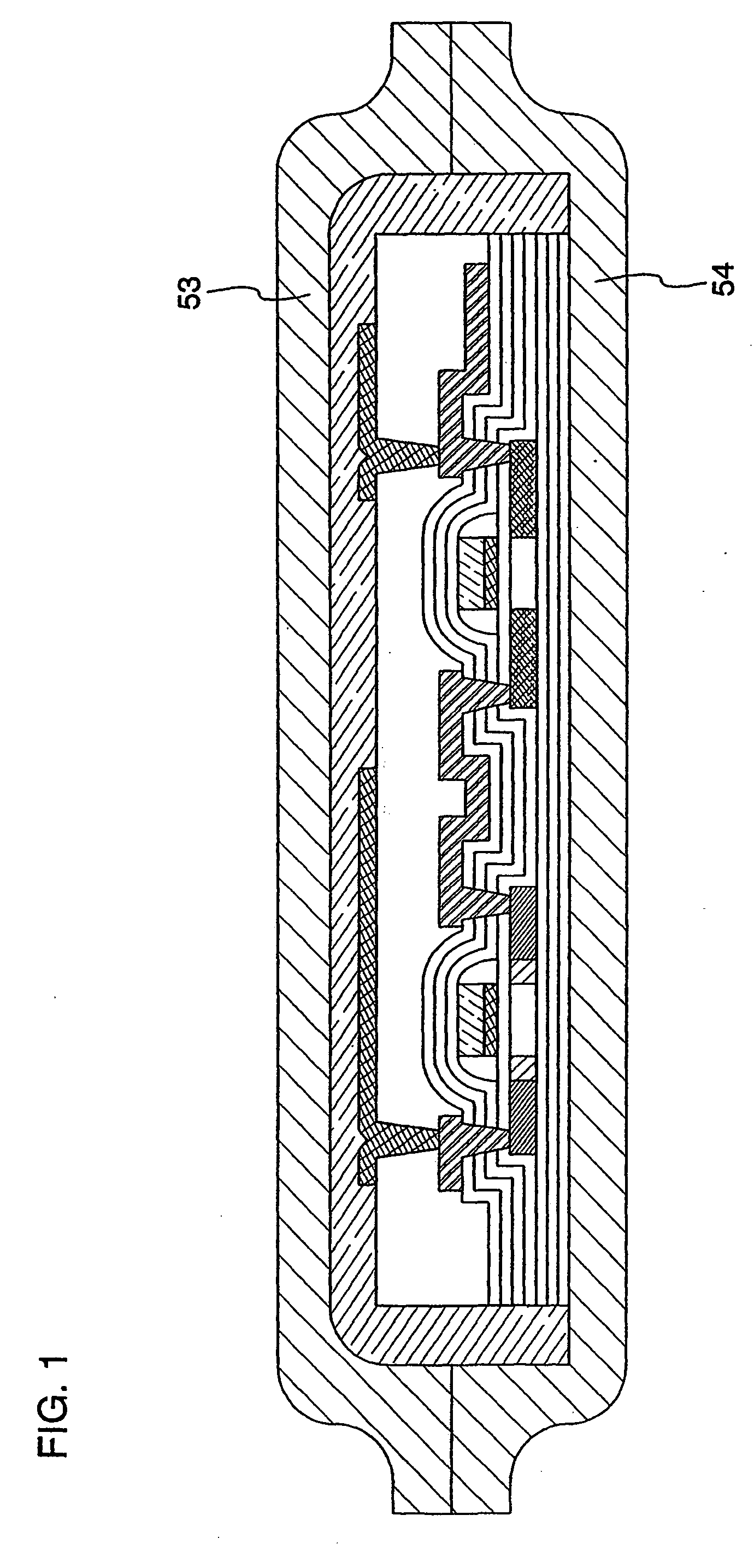
Wireless Chip And Manufacturing Method Thereof
a technology of wireless chips and manufacturing methods, applied in the field of wireless chips, can solve the problems of difficult mass production, difficult to reduce the cost of a wireless chip, and difficult to reduce and achieve the effect of reducing the cost of a wireless chip and being easy to process into a flexible shap
- Summary
- Abstract
- Description
- Claims
- Application Information
AI Technical Summary
Benefits of technology
Problems solved by technology
Method used
Image

Examples
embodiment 1
[0100] In this embodiment, seven samples each used as a peeling layer are formed (see Table 1). The temperature dependence of the etching rate when these samples are etched with the use of a chlorine trifluoride (ClF3) gas is examined. The experimental result is explained with reference to FIG. 25.
TABLE 1treatment forfilmforming metalthicknessresistivity——oxide film(nm)(Om)sample1tungsten oxide layer (WOx)—4004.20E−04sample2stacked layer structure of550° C.50˜1002.20E−05tungsten layer (W; lower layer)10 min and tungsten oxide layer (WOx;upper layer)sample3stacked layer structure of450° C.50˜1001.50E−05tungsten layer (W; lower layer)4 minand tungsten oxide layer (WOx;upper layer)sample4tungsten layer (W)—501.40E−05sample5silicon layer (Si)—50—sample6silicon layer (Si)—50—sample7tungsten oxide layer (WO3)650° C.70˜100—2 min
[0101] A method for manufacturing a peeling layer of Samples 1 to 7 is explained below in detail. In Sample 1, a tungsten oxide layer (WOx) is formed in an argon ...
embodiment 2
[0111] According to the above embodiment mode, the peeling layer 11 is removed by etchant completely in order to peel the thin film integrated circuit 52 from the substrate 10 (see FIG. 11). However, the present invention is not limited to this embodiment mode and a peeling layer 11 may be removed selectively instead of removing completely by introducing etchant to openings (see FIG. 18A). Then, after removing the peeling layer 11 selectively, a thin film integrated circuit 52 may be peeled from the substrate 10 by a physical means (physical force) (see FIG. 18B). Note that peeling the thin film integrated circuit 52 by a physical means (physical force) means to peel it by externally applying such a stress as a wind pressure of gas blown from a nozzle or an ultrasonic wave. When the thin film integrated circuit 52 is peeled by a physical means (physical force), the peeling layer 11 may be left over the substrate 10 or both the peeling layer 11 and the thin film integrated circuit 52...
embodiment 3
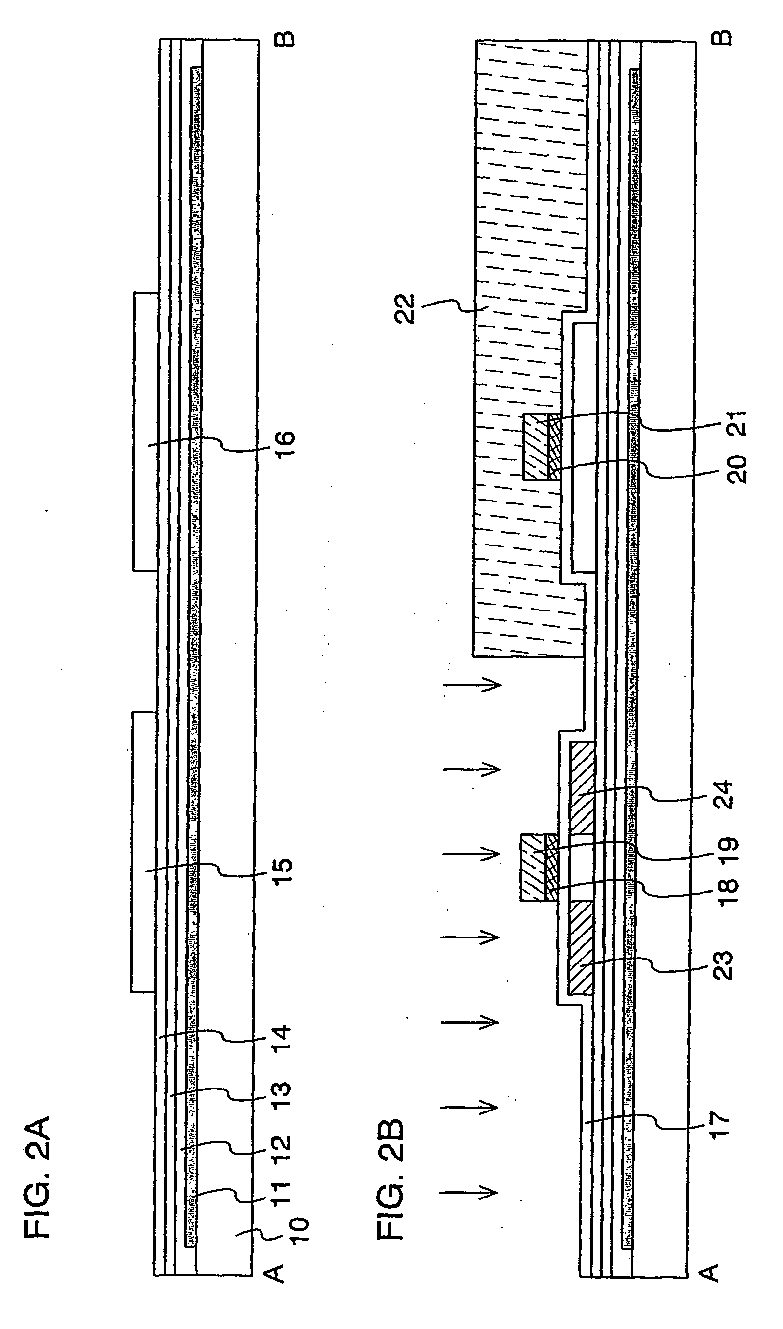
[0113] This embodiment will explain a process of forming a minute gate electrode. First, a peeling layer 11, insulating layers 12 to 14, and crystalline semiconductor layers 15 and 16 are formed over a substrate 10 having the insulating surface (see FIG. 19A). Next, conductive layers 70 and 71 are formed over the entire surface (see FIG. 19A). Then, resist masks 72 and 73 are formed over the conductive layer 71 by using a photomask. Subsequently, the resist masks 72 and 73 are etched by a known etching treatment such as oxygen plasma treatment to form new resist masks 74 and 75 (see FIG. 19B). The resist masks 74 and 75 through the above processes can be formed so minute that a limitation in which a resist mask can be formed by a photolithography method is exceeded. When etching treatment is performed by using the resist masks 74 and 75, a minute gate electrode can be formed.
[0114] In addition, first, resist masks 72 and 73 are formed by using a photolithography method as a method ...
PUM
 Abstract
Description
Claims
Application Information